- 您現(xiàn)在的位置:買(mǎi)賣(mài)IC網(wǎng) > PDF目錄385403 > HT7627 (Holtek Semiconductor Inc.) PFM Step-up DC/DC Converter & Voltage Detector PDF資料下載
參數(shù)資料
| 型號(hào): | HT7627 |
| 廠(chǎng)商: | Holtek Semiconductor Inc. |
| 英文描述: | PFM Step-up DC/DC Converter & Voltage Detector |
| 中文描述: | PFM步升直流/直流轉(zhuǎn)換器 |
| 文件頁(yè)數(shù): | 3/6頁(yè) |
| 文件大小: | 77K |
| 代理商: | HT7627 |

HT7627
Rev. 1.00
3
January 18, 2002
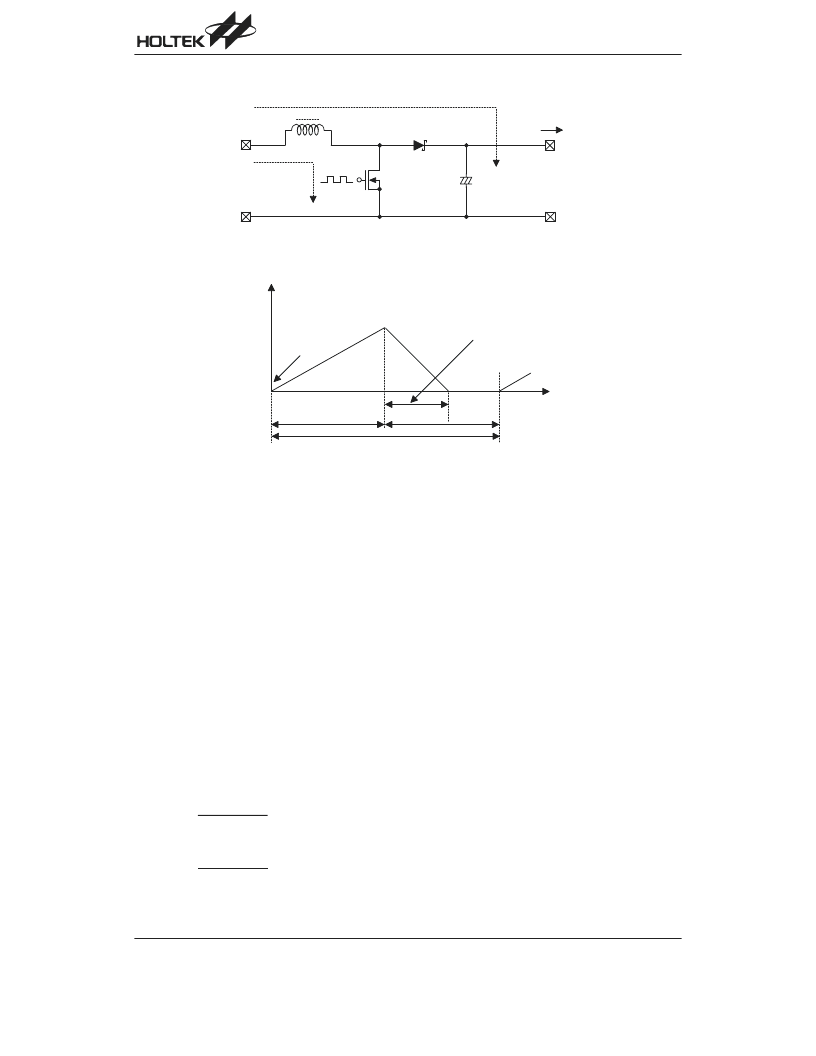
The operation will be explained with reference to the following diagrams:
Step1: t
r
is turned ON and current I
L
(=i1) flows, so that energy is charged in L. At this moment, I
L
(=i1) is increased
from I
Lmin
to reach I
Lmax
in proportion to the on-time period (t
on
) of t
r
.
Step2: When t
r
is turned OFF, Schottky diode (SD) is turned ON in order that L maintains I
L
at I
Lmax
, so that current I
L
(=i2) is released.
Step3: I
L
(=i2) is gradually decreased, I
L
reaches I
Lmin
after a time period of t
open
, so that SD is turned OFF. t
r
will be
turned ON in the next cycle.
In the case of PWM control system, the output voltage is maintained constant by controlling the on-time period (t
on
),
with the oscillator frequency (f
OSC
) being maintained constant.
Voltage detector operation
The HT7627 built-in voltage detector is equipped with a high stability voltage reference which is connected to the nega-
tive of a comparator
denoted as Vref in the following figure for NMOS output voltage detector.
When the voltage drop to the positive input of the comparator (i.e. V
B
) is higher than Vref, V
OUT
goes high, and V
B
is ex-
pressed as V
BH
=V
DD
(R
B
+R
C
) / (R
A
+R
B
+R
C
). If V
DD
is decreased so that V
B
falls to a value less than Vref, the com-
parator output inverts from high to low, V
OUT
goes low, V
C
is high, RC is bypassed, and V
B
becomes: V
BL
=V
DD
R
B
/(R
A
+R
B
), which is less than V
BH
. By so doing, the comparator output will remain low to prevent the circuit from oscil-
lating when V
B
Vref.
If V
DD
falls below the minimum operating voltage, the output becomes undefined. When V
DD
goes from low to V
DD
/ (R
A
+R
B
) > Vref, the comparator output and V
OUT
goes high. The detectable voltage is defined as:
R
B
V
DETECT
( )=
R
R
R
R
R
A
B
C
B
C
Vref
The release voltage is defined as:
V
DETECT
(+)=
R
R
R
R
A
B
C
B
Vref
) (
"
)
)
)
)
*
+ " ,
相關(guān)PDF資料 |
PDF描述 |
|---|---|
| HT7660 | CMOS Switched-Capacitor Voltage Converter(CMOS可變電容變壓器) |
| HT7700 | Key & Touch Linear Dimmer |
| HT7700A | Key & Touch Linear Dimmer |
| HT7700B | Key & Touch Linear Dimmer |
| HT7700C | Key & Touch Linear Dimmer |
相關(guān)代理商/技術(shù)參數(shù) |
參數(shù)描述 |
|---|---|
| HT7627-8SOP-A | 制造商:HOLTEK 制造商全稱(chēng):Holtek Semiconductor Inc 功能描述:Analog IC |
| HT7630(16DIP) | 制造商:未知廠(chǎng)家 制造商全稱(chēng):未知廠(chǎng)家 功能描述:Motion/Proximity Detector |
| HT7630(16SOIC) | 制造商:未知廠(chǎng)家 制造商全稱(chēng):未知廠(chǎng)家 功能描述:Motion/Proximity Detector |
| HT7660 | 制造商:HOLTEK 制造商全稱(chēng):Holtek Semiconductor Inc 功能描述:CMOS Switched-Capacitor Voltage Converter |
| HT7660(8DIP) | 制造商:未知廠(chǎng)家 制造商全稱(chēng):未知廠(chǎng)家 功能描述:DC-to-DC Voltage Converter |
發(fā)布緊急采購(gòu),3分鐘左右您將得到回復(fù)。