- 您現(xiàn)在的位置:買賣IC網(wǎng) > PDF目錄371884 > HS1-80C85RH (Intersil Corporation) Radiation Hardened 8-Bit CMOS Microprocessor PDF資料下載
參數(shù)資料
| 型號(hào): | HS1-80C85RH |
| 廠商: | Intersil Corporation |
| 英文描述: | Radiation Hardened 8-Bit CMOS Microprocessor |
| 中文描述: | 輻射加固8位CMOS微處理器 |
| 文件頁數(shù): | 14/19頁 |
| 文件大小: | 159K |
| 代理商: | HS1-80C85RH |
14
HS-80C85RH
HS-80C85RH Caveats
1. An important caveat that is applicable to CMOS devices in gen-
eral is that unused inputs should never be left floating. This rule
also applies to inputs connected to a tri- state bus. The need for
external pull-up resistors during tri-state bus conditions is elimi-
nated by the presence of regenerative latches on the following
HS-80C85RH output pins: AD0-AD7, A8-A15, and IO/M. Figure
10 depicts an output and corresponding regenerative latch.
When the output driver assumes the high impedance state, the
latch holds the bus in whatever logic state (high or low) it was be-
fore the tri-state condition. A transient drive current of approxi-
mately
±
1.0mA at 0.5 VDD for 10nsec is required to switch the
latch. Thus, CMOS device inputs connected to the bus are not
allowed to float during tri-state conditions.
2. The RD and WR pins of the HS-80C85RH contain internal dy-
namic pull-up transistors to avoid spurious selection of memory
devices when the RD and WR pins assume the high impedance
state. This eliminates the need for external resistive pull-ups on
these pins.
3. The RESET IN and X1 inputs on the HS-80C85RH are schmit
trigger inputs. This eliminates the possibility of internal oscilla-
tions in response to slow rise time input signals at these pins.
4. A high frequency bypass capacitor of approximately 0.1
μ
F
should be connected between VDD and GND to shunt power
supply transients.
5. The HS-80C85RH is functional within 10 input clock cycles after
application of power (assuming that reset has been asserted
from power-on). Start up conditions in the crystal controlled
oscillator mode must also account for the characteristics of the
oscillator.
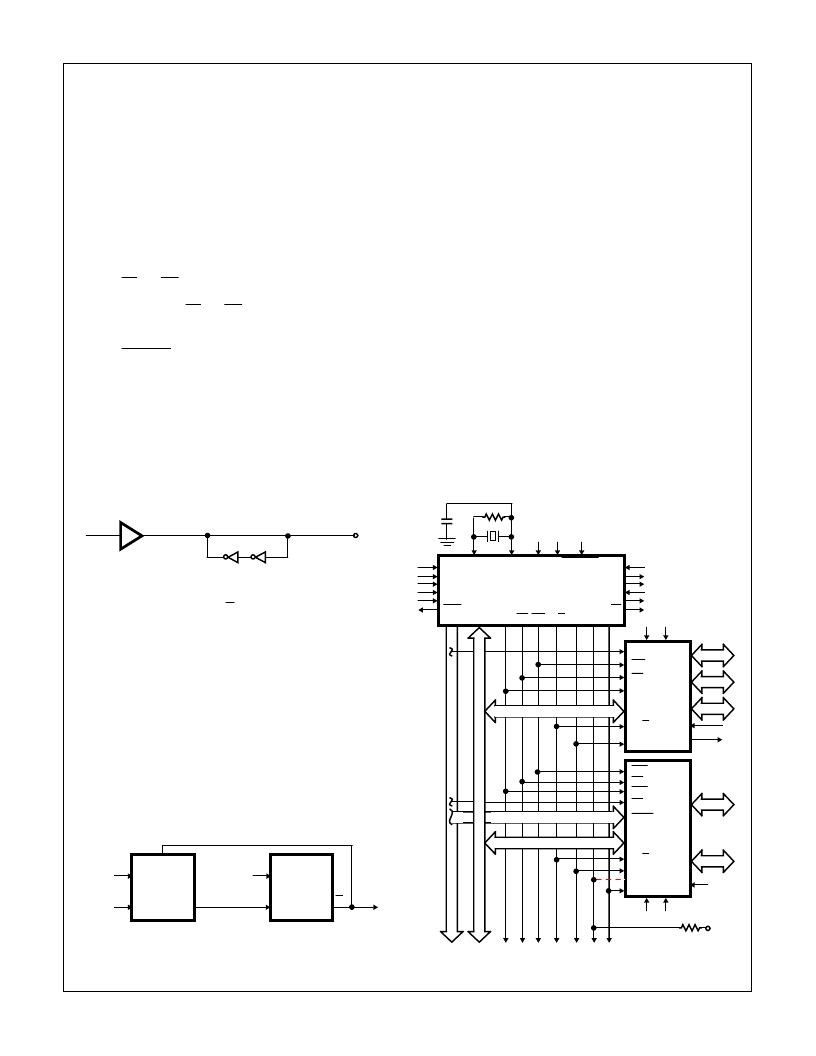
Generating An HS-80C85RH Wait State
If your system requirements are such that slow memories or
peripheral devices are being used, the circuit shown in
Figure 11 may be used to insert one WAIT state in each
HS-80C85RH machine cycle.
The D flip-flops should be chosen so that:
1. CLK is rising edge-triggered
2. CLEAR is low-level active.
The READY line is used to extend the read and write pulse
lengths so that the 80C85RH can be used with slow mem-
ory. HOLD causes the CPU to relinquish the bus when it is
through with it by floating the Address and Data Buses.
FIGURE 10. OUTPUT DRIVER AND LATCH FOR PINS ADO-AD7,
A8-A15 AND IO/M.
FIGURE 11. GENERATION OF A WAIT STATE FOR HS-80C85RH
CPU.
OUTPUT
DRIVER
REGENERATIVE
LATCH
OUTPUT
PIN
CLEAR
CLK
“D”
F/F
D
ALE
VDD
80C85RH
CLK
OUTPUT
Q
TO
80C85RH
READY
INPUT
CLK
“D”
F/F
D
Q
ALE and CLK (OUT) should be buffered if CLK
input of latch exceeds 80C85RH IOL or IOH.
System Interface
The HS-80C85RH family includes memory components,
which are directly compatible to the HS-8OC8SRH CPU. For
example, a system consisting of the three radiation-
hardened
chips,
HS-80C85RH,
HS-83C55RH will have the following features:
1. 2K Bytes ROM
2. 256 Bytes RAM
3. 1 Timer/Counter
4. 4 8-bit I/O Ports
5. 1 6-bit I/O Port
6. 4 Interrupt Levels
7. Serial In/Serial Out Ports
This minimum system, using the standard I/O technique is
as shown in Figure 12.
HS-81C56RH,
and
In addition to standard 1/0, the memory mapped I/O offers
an efficient I/O addressing technique. With this technique, an
area of memory address space is assigned for I/O address,
thereby, using the memory address for I/O manipulation.
Figure 13 shows the system configuration of Memory
Mapped I/O using HS-80C85RH.
The HS-80C85RH CPU can also interface with the standard
radiation-hardened memory that does not have the
multiplexed address/data bus. It will require use of the
HS-82C12RH (8-bit latch) as shown in Figure 14.
FIGURE 12. HS-80C85RH MINIMUM SYSTEM (STANDARD I/O
TECHNIQUE)
TRAP
RST 7.5
RST 6.5
RST 5.5
INTR
INTA
ADDR
ADDR/
DATA
ALE RD WR IO/M
RDYCLK
X2
X1
HOLD
HLDA
SOD
SID
S1
S0
RESET IN
HS-80C85RH
VSS VDD
VSS VDD
CE
WR
RD
ALE
DATA/
ADDR
IO/M
RESET
PORT
A
PORT
B
PORT
C
IN
TIMER
OUT
(8)
(8)
(6)
(8)
(8)
IOW
RD
ALE
CE
DATA/
ADDR
IO/M
RESET
RDY
CLK
PORT
A
PORT
B
(8)
(8)
A0-10
IOR
VDD
VDD
VSS VDD
Optional Connection
OUT
H
H
Spec Number
518054
相關(guān)PDF資料 |
PDF描述 |
|---|---|
| HS9-80C85RH | Radiation Hardened 8-Bit CMOS Microprocessor |
| HS-OP470AR | 16 AMP SPDT MINIATURE POWER RELAY |
| HS-OP470ARH | Radiation Hardened, Very Low Noise Quad Operational Amplifier(抗輻射低噪聲四路運(yùn)算放大器) |
| HS9-OP470ARH | Radiation Hardened, Very Low Noise Quad Operational Amplifier |
| HS9-OP470ARH-Q | Radiation Hardened, Very Low Noise Quad Operational Amplifier |
相關(guān)代理商/技術(shù)參數(shù) |
參數(shù)描述 |
|---|---|
| HS1-80C85RH-8 | 制造商:INTERSIL 制造商全稱:Intersil Corporation 功能描述:Radiation Hardened 8-Bit CMOS Microprocessor |
| HS1-80C85RH-Q | 制造商:INTERSIL 制造商全稱:Intersil Corporation 功能描述:Radiation Hardened 8-Bit CMOS Microprocessor |
| HS1-80C86RH | 制造商:INTERSIL 制造商全稱:Intersil Corporation 功能描述:Radiation Hardened 16-Bit CMOS Microprocessor |
| HS1-80C86RH/PROTO | 制造商:未知廠家 制造商全稱:未知廠家 功能描述:Microprocessor |
| HS1-80C86RH-8 | 制造商:Intersil Corporation 功能描述:MPU 16BIT CMOS 5MHZ 40PIN SBCDIP - Rail/Tube |
發(fā)布緊急采購,3分鐘左右您將得到回復(fù)。