- 您現(xiàn)在的位置:買賣IC網(wǎng) > PDF目錄370623 > HM5425801BTT-75A (ELPIDA MEMORY INC) 256M SSTL_2 interface DDR SDRAM 143 MHz/133 MHz/125 MHz/100 MHz 4-Mword 】 16-bit 】 4-bank/8-Mword 】 8-bit 】 4-bank/ 16-Mword 】 4-bit 】 4-bank PDF資料下載
參數(shù)資料
| 型號(hào): | HM5425801BTT-75A |
| 廠商: | ELPIDA MEMORY INC |
| 元件分類: | DRAM |
| 英文描述: | 256M SSTL_2 interface DDR SDRAM 143 MHz/133 MHz/125 MHz/100 MHz 4-Mword 】 16-bit 】 4-bank/8-Mword 】 8-bit 】 4-bank/ 16-Mword 】 4-bit 】 4-bank |
| 中文描述: | 32M X 8 DDR DRAM, 0.75 ns, PDSO66 |
| 封裝: | 0.400 INCH, PLASTIC, TSOP2-66 |
| 文件頁數(shù): | 26/65頁 |
| 文件大小: | 489K |
| 代理商: | HM5425801BTT-75A |
第1頁第2頁第3頁第4頁第5頁第6頁第7頁第8頁第9頁第10頁第11頁第12頁第13頁第14頁第15頁第16頁第17頁第18頁第19頁第20頁第21頁第22頁第23頁第24頁第25頁當(dāng)前第26頁第27頁第28頁第29頁第30頁第31頁第32頁第33頁第34頁第35頁第36頁第37頁第38頁第39頁第40頁第41頁第42頁第43頁第44頁第45頁第46頁第47頁第48頁第49頁第50頁第51頁第52頁第53頁第54頁第55頁第56頁第57頁第58頁第59頁第60頁第61頁第62頁第63頁第64頁第65頁
HM5425161B, HM5425801B, HM5425401B Series
Data Sheet E0086H20
26
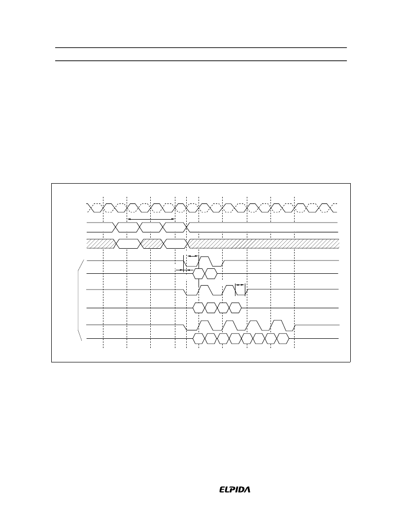
Write operation
: The burst length (BL) and the burst type (BT) of the mode register are referred when a
write command is issued. The burst length (BL) determines the length of a sequential data input by the write
command which can be set to 2, 4, or 8. The latency from write command to data input is fixed to 1. The
starting address of the burst read is defined by the column address (AY0 to AY8; the HM5425161B, AY0 to
AY9; the HM5425801B, AY0 to AY9, AY11; the HM5425401B), the bank select address (BA0/BA1) which
are loaded via the A0 to A12, BA0 to BA1 pins in the cycle when the write command is issued. DQS,
DQSU/DQSL should be input as the strobe for the input-data and DM, DMU/DML as well during burst
operation. t
WPREH
prior to the first rising edge of the DQS, the DQSU/DQSL should be set to Low and t
WPST
after the last falling edge of the data strobe can be set to High-Z. The leading low period of DQS is referred
as write preamble. The last low period of DQS is referred as wrtie postamble.
Write Operation
in1
in0
in1
in2
in3
in0
in1
in2
in3
in4
in5
in6
in7
CLK
CLK
Address
DQS*
Din
BL = 2
BL = 4
BL = 8
Command
BL: Burst length
t1
t0
t2
t3
t3.5
t4
t5
t6
t7
t8
t
RCD
t
WPST
DQS*:DQS,DQSU/DQSL
in0
ACTV
NOP
NOP
NOP
WRITE
t
WPREH
t
WPRES
Row
Column
發(fā)布緊急采購,3分鐘左右您將得到回復(fù)。