- 您現(xiàn)在的位置:買賣IC網(wǎng) > PDF目錄371830 > HM1-6551883 (Intersil Corporation) 256 x 4 CMOS RAM PDF資料下載
參數(shù)資料
| 型號: | HM1-6551883 |
| 廠商: | Intersil Corporation |
| 英文描述: | 256 x 4 CMOS RAM |
| 中文描述: | 256 × 4 CMOS存儲器 |
| 文件頁數(shù): | 1/9頁 |
| 文件大?。?/td> | 116K |
| 代理商: | HM1-6551883 |
6-101
March 1997
HM-6551/883
256 x 4 CMOS RAM
Features
This Circuit is Processed in Accordance to MIL-STD-
883 and is Fully Conformant Under the Provisions of
Paragraph 1.2.1.
Low Power Standby. . . . . . . . . . . . . . . . . . . . 50
μ
W Max
Low Power Operation . . . . . . . . . . . . . 20mW/MHz Max
Fast Access Time. . . . . . . . . . . . . . . . . . . . . .220ns Max
Data Retention . . . . . . . . . . . . . . . . . . . . . . . .at 2.0V Min
TTL Compatible Input/Output
High Output Drive - 1 TTL Load
Internal Latched Chip Select
High Noise Immunity
On-Chip Address Register
Latched Outputs
Three-State Output
Description
The HM-6551/883 is a 256 x 4 static CMOS RAM fabricated
using self-aligned silicon gate technology. Synchronous cir-
cuit design techniques are employed to achieve high perfor-
mance and low power operation. On chip latches are
provided for address and data outputs allowing efficient
interfacing with microprocessor systems. The data output
buffers can be forced to a high impedance state for use in
expanded memory arrays.
The HM-6551/883 is a fully static RAM and may be main-
tained in any state for an indefinite period of time. Data
retention supply voltage and supply current are guaranteed
over temperature.
Ordering Information
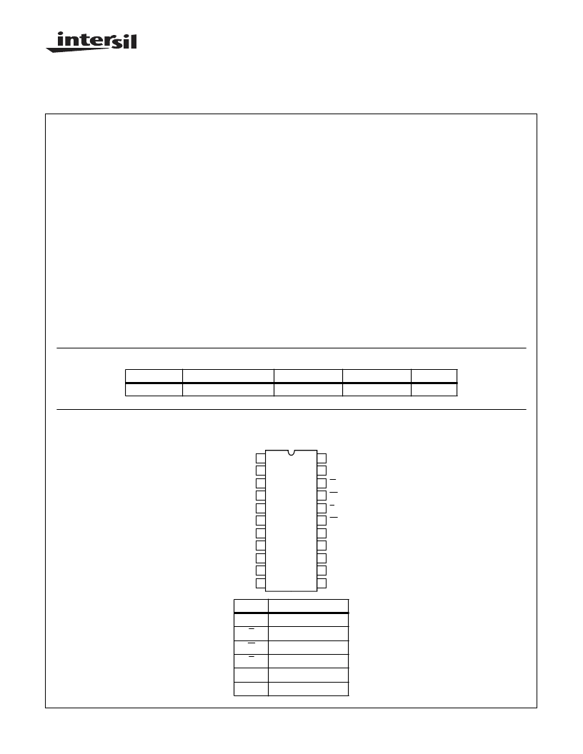
Pinout
HM-6551/883 (CERDIP)
TOP VIEW
PACKAGE
TEMPERATURE RANGE
-55
o
C to +125
o
C
220ns
300ns
PKG. NO.
CERDIP
HM-6551B/883
HM1-6551/883
F22.4
PIN
DESCRIPTION
A
Address Input
E
Chip Enable
W
Write Enable
S
Chip Select
D
Data Input
Q
Data Output
1
22
12
13
14
15
16
17
18
19
21
20
11
10
9
8
7
6
5
3
2
A2
A1
A0
A5
A6
A7
D0
GND
Q0
D1
A4
Q3
D3
Q2
D2
Q1
4
A3
VCC
W
S1
E
S2
File Number
2988.1
CAUTION: These devices are sensitive to electrostatic discharge; follow proper IC Handling Procedures.
http://www.intersil.com or 407-727-9207
|
Copyright
Intersil Corporation 1999
相關(guān)PDF資料 |
PDF描述 |
|---|---|
| HM-65642 | RES,Metal Film,100KOhms,500WV,1+/-% Tol,-50,50ppm-TC |
| HM-65642883 | 8K x 8 Asynchronous CMOS Static RAM |
| HM1-65642883 | 8K x 8 Asynchronous CMOS Static RAM |
| HM1-65642B883 | 8K x 8 Asynchronous CMOS Static RAM |
| HM1-65642C883 | 8K x 8 Asynchronous CMOS Static RAM |
相關(guān)代理商/技術(shù)參數(shù) |
參數(shù)描述 |
|---|---|
| HM1-6551-9 | 制造商:Rochester Electronics LLC 功能描述:- Bulk |
| HM1-6551B/883 | 制造商:Intersil Corporation 功能描述:SRAM ASYNC SGL 5V 1KBIT 256 X 4 220NS 22CDIP - Rail/Tube |
| HM1-6551B-8 | 制造商:未知廠家 制造商全稱:未知廠家 功能描述:x4 Synchronous SRAM |
| HM1-6551B-9 | 制造商:Rochester Electronics LLC 功能描述:- Bulk |
| HM1-6561/883 | 制造商:INTERSIL 制造商全稱:Intersil Corporation 功能描述:256 x 4 CMOS RAM |
發(fā)布緊急采購,3分鐘左右您將得到回復(fù)。