- 您現(xiàn)在的位置:買賣IC網(wǎng) > PDF目錄384423 > HIP9022AM (INTERSIL CORP) Dual High Speed Laser Driver PDF資料下載
參數(shù)資料
| 型號: | HIP9022AM |
| 廠商: | INTERSIL CORP |
| 元件分類: | 其它接口 |
| 英文描述: | Dual High Speed Laser Driver |
| 中文描述: | SPECIALTY INTERFACE CIRCUIT, PQCC68 |
| 封裝: | PLASTIC, MS-018AE, LCC-68 |
| 文件頁數(shù): | 6/10頁 |
| 文件大小: | 98K |
| 代理商: | HIP9022AM |
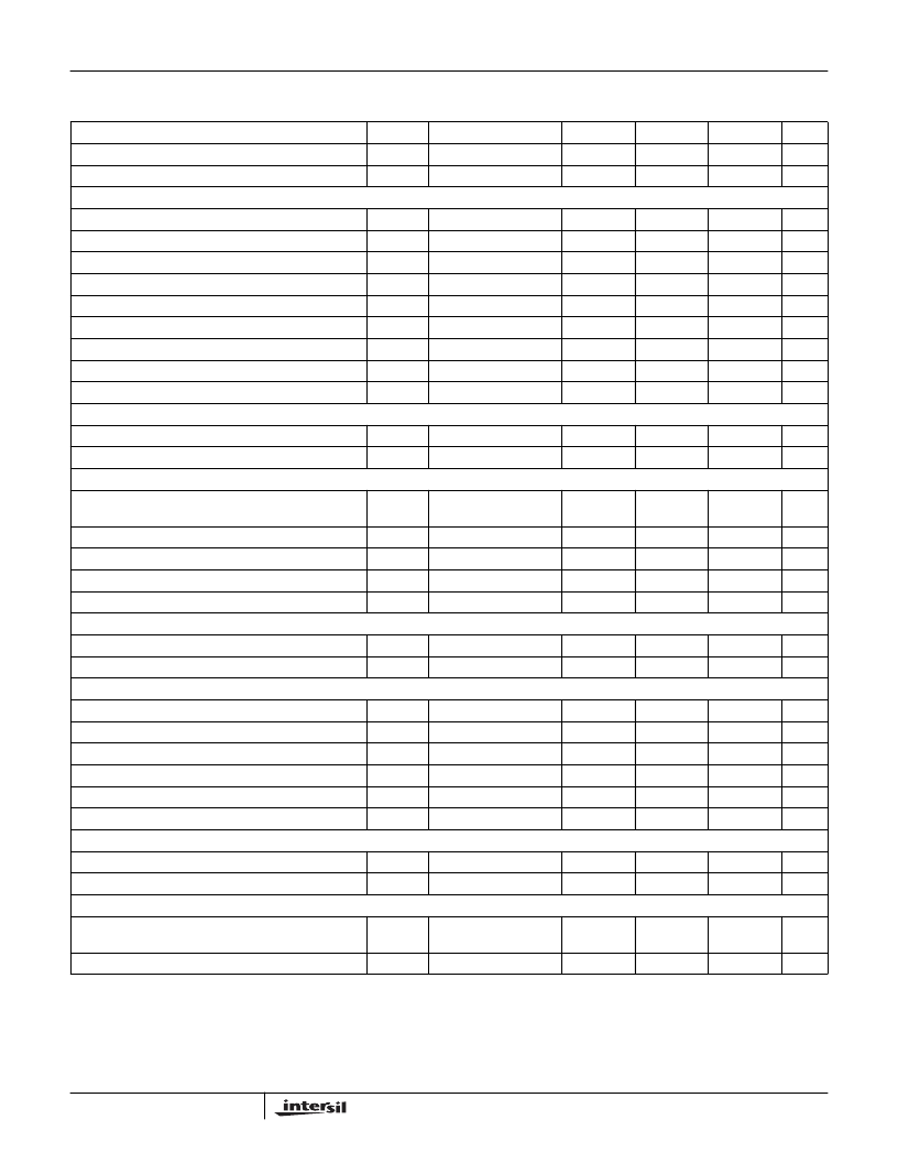
4-6
Driver Maximum Output Current
I
DRSW
f
SC
-1
-
1
A
Shunt Controller Switching Frequency
0
-
2.5
MHz
ANALOG SAMPLE/HOLD AMPLIFIERS
Low Level Input Voltage
V
IL
I
IL
V
IH
V
HYS
V
IN
0
-
1.5
V
Low Level Input Current
-140
-
-
μ
A
High Level Input Voltage
3.5
-
V
CC
+ 0.3
-
V
Minimum Hysteresis
0.3
-
V
Analog Input Voltage Range
0
-
V
CC
- 0.2
-
V
Minimum Sample/Hold Pulse Width
-
10
μ
s
Droop Rate, Constant Current Addresses #’s 1, 2
-
-
0.006
V/s
Droop Rate, Other Addresses #’s 3 - 8
-
-
0.06
V/s
Maximum Analog Multiplexing Frequency
-
-
30
kHz
DIAGNOSTIC OUTPUT
(DIAG Output)
Voltage Follower Voltage Range
V
O
V
CL
0
-
V
CC
- 0.2
V
CC
+ 0.3
V
Voltage Follower Maximum Clamp Voltage
-
-
V
O. C. (OVER CURRENT) COMPARATOR
(OC1, 2 Outputs)
Threshold (%) O.C. Detection
Programmed Current
as Ref.
-
140
-
%
Output Voltage, Low Level
V
OL
I
OL
V
OH
I
OH
0
-
1.5
V
Output Current, Low Level
-
12
-
mA
Output Voltage, High Level
3.5
-
V
CC
- 0.5
-
V
Output Current, High Level
-
4
mA
TEC REF. RESISTOR AND DRIVE OUTPUT
TECREFR Output Voltage to Reference Resistor
V
REFR
V
TECG
1.71
1.9
2.09
V
TECGDR1, 2 Drive Output Voltage
0
-
9
V
OVER/UNDER TEMPERATURE COMPARATOR
(To OT Output)
Under Temp. Limit
T
LOW
T
HIGH
V
OL
I
OL
V
OH
I
OH
2.07
2.1
2.13
V
Over Temp. Limit
1.67
1.7
1.73
V
Output Voltage, Low Level
0
-
1.5
V
Output Current, Low Level
-
12
-
mA
Output Voltage, High Level
3.5
-
V
CC
- 0.5
-
V
Output Current, High Level
-
4
mA
RELAY DRIVER
Driver Output Current
I
RLY
r
DS(ON)
-
-
30
mA
Drain to Source Resistance
-
20
-
LASER PROTECTION DIODES
See Figure 1
Maximum Diode Forward Voltage Drop
V
LDX,
V
ESDX
I
LDX
10A Peak Current
-
-
2
V
Maximum Reverse Diode Current
-
-
1
μ
A
NOTE:
2. The drive control sets the high and low voltages to the gate of the Power FET driver (shunt switch). Both the upper and lower levels are set by
values held in two of the sample/hold amplifiers. External capacitors at VUP1, 2 and VLOW1, 2 are required for stabilization.
Electrical Specifications
T
J
= 100
ο
C, V
DD
= 12V, V
CC
= 5V, V
EE
= -5V, INVERT Low (Figure 1 Configuration)
Unless Otherwise Specified
(Continued)
PARAMETER
SYMBOL
TEST CONDITIONS
MIN
TYP
MAX
UNITS
HIP9022
相關PDF資料 |
PDF描述 |
|---|---|
| HIRF740 | N-Channel Power MOSFET (400V, 10A) |
| HIRF740F | N-Channel Power MOSFET (400V, 10A) |
| HJ45H11 | PNP EPITAXIAL PLANAR TRANSISTOR |
| HK-1005-18NJTK | Surface Mount Ferrite Products |
| HK-0603-10NJTK | Surface Mount Ferrite Products |
相關代理商/技術參數(shù) |
參數(shù)描述 |
|---|---|
| HIPC6100 | 制造商:Hubbell Wiring Device-Kellems 功能描述:CABLE, HI-IMPACT,C6,BK,100FT |
| HIPE200W//GLASSGUARD | 制造商:VENTURE LIGHTING EUROPE LTD 功能描述:SHATTERPROOF LAMP 200W |
| HIPMP-RJ11 | 制造商:Belden Inc 功能描述:PLUG RJ11 w/50 MICRON |
| HIPMP-RJ45 | 制造商:Belden Inc 功能描述:PLUG, RJ45 w/50 MICRON |
| HIPMP-RJ45CAT6 | 制造商:Belden Inc 功能描述:MOD.PLUG, RJ45/CAT6,8P8C,UL |
發(fā)布緊急采購,3分鐘左右您將得到回復。