- 您現(xiàn)在的位置:買賣IC網(wǎng) > PDF目錄385382 > HIP6014CB (INTERSIL CORP) Buck and Synchronous-Rectifier (PWM) Controller and Output Voltage Monitor PDF資料下載
參數(shù)資料
| 型號: | HIP6014CB |
| 廠商: | INTERSIL CORP |
| 元件分類: | 穩(wěn)壓器 |
| 英文描述: | Buck and Synchronous-Rectifier (PWM) Controller and Output Voltage Monitor |
| 中文描述: | 0.5 A SWITCHING CONTROLLER, 1000 kHz SWITCHING FREQ-MAX, PDSO20 |
| 封裝: | PLASTIC, MS-013AC, SOIC-20 |
| 文件頁數(shù): | 7/12頁 |
| 文件大小: | 211K |
| 代理商: | HIP6014CB |

7
Remove input power before changing the output voltage.
Adjusting the output voltage during operation could toggle
the PGOOD signal and exercise the overvoltage protection.
All VID pin combinations resulting in a 0V output setting
activate the Power-On Reset function and disable the gate
drive circuitry. For these specific VID combinations, though,
PGOOD asserts a high level. This unusual behavior has
been implemented in order to allow for operation in dual-
microprocessor systems by AND-ing the PGOOD signals
from the two individual power converters.
Application Guidelines
Layout Considerations
As in any high frequency switching converter, layout is very
important. Switching current from one power device to another
can generate voltage transients across the impedances of the
interconnecting bond wires and circuit traces. These
interconnecting impedances should be minimized by using
wide, short printed circuit traces. The critical components
should be located as close together as possible, using ground
plane construction or single point grounding.
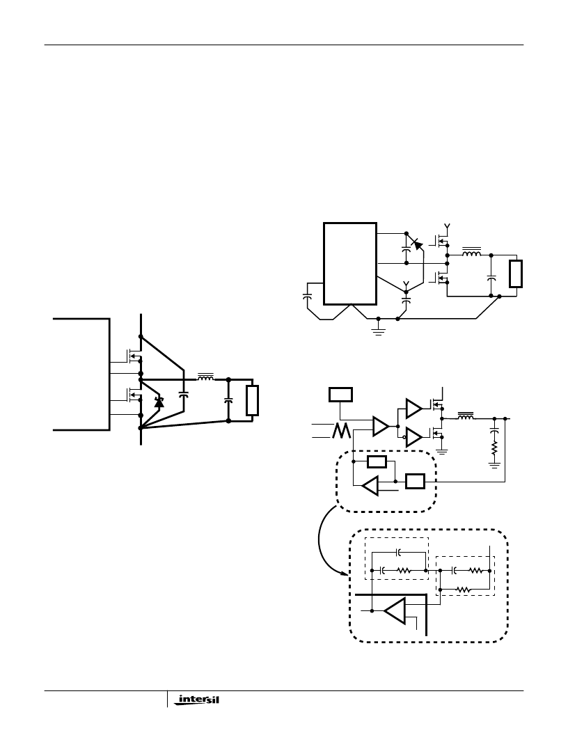
Figure 5 shows the critical power components of the
converter. To minimize the voltage overshoot the
interconnecting wires indicated by heavy lines should be
part of ground or power plane in a printed circuit board. The
components shown in Figure 5 should be located as close
together as possible. Please note that the capacitors C
IN
and C
O
each represent numerous physical capacitors.
Locate the HIP6014 within 3 inches of the MOSFETs, Q
1
and Q
2
. The circuit traces for the MOSFETs’ gate and
source connections from the HIP6014 must be sized to
handle up to 1A peak current.
Figure 6 shows the circuit traces that require additional
layout consideration. Use single point and ground plane
construction for the circuits shown. Minimize any leakage
current paths on the SS PIN and locate the capacitor, C
SS
close to the SS pin because the internal current source is
only 10
μ
A. Provide local V
CC
decoupling between V
CC
and
GND pins. Locate the capacitor, C
BOOT
as close as practical
to the BOOT and PHASE pins.
Feedback Compensation
Figure 7 highlights the voltage-mode control loop for a
synchronous-rectified buck converter. The output voltage
(V
OUT
) is regulated to the Reference voltage level. The error
amplifier (Error Amp) output (V
E/A
) is compared with the
oscillator (OSC) triangular wave to provide a pulse-width
modulated (PWM) wave with an amplitude of V
IN
at the
PHASE node. The PWM wave is smoothed by the output filter
(L
O
and C
O
).
PGND
L
O
C
O
LGATE
UGATE
PHASE
Q
1
Q
2
D
2
V
IN
V
OUT
RETURN
HIP6014
C
IN
L
FIGURE 5. PRINTED CIRCUIT BOARD POWER AND
GROUND PLANES OR ISLANDS
FIGURE 6. PRINTED CIRCUIT BOARD SMALL SIGNAL
LAYOUT GUIDELINES
+12V
HIP6014
SS
GND
V
CC
BOOT
D
1
L
O
C
O
V
OUT
L
Q
1
Q
2
PHASE
+V
IN
C
BOOT
C
VCC
C
SS
FIGURE 7. VOLTAGE-MODE BUCK CONVERTER
COMPENSATION DESIGN
V
OUT
REFERENCE
L
O
C
O
ESR
V
IN
V
OSC
ERROR
AMP
PWM
DRIVER
(PARASITIC)
Z
FB
+
-
DACOUT
R
1
R
3
R
2
C
3
C
2
C
1
COMP
V
OUT
FB
Z
FB
HIP6014
Z
IN
COMPARATOR
DRIVER
DETAILED COMPENSATION COMPONENTS
PHASE
V
E/A
+
-
+
-
Z
IN
OSC
HIP6014
相關(guān)PDF資料 |
PDF描述 |
|---|---|
| HIP6016 | FPGA - 100000 SYSTEM GATE 2.5 VOLT - NOT RECOMMENDED for NEW DESIGN |
| HIP6016CB | Advanced PWM and Dual Linear Power Control |
| HIP6017B | FPGA - 100000 SYSTEM GATE 2.5 VOLT - NOT RECOMMENDED for NEW DESIGN |
| HIP6017BCB | FPGA - 100000 SYSTEM GATE 2.5 VOLT - NOT RECOMMENDED for NEW DESIGN |
| HIP6018B | 100,000 System Gate FPGA - NOT RECOMMENDED for NEW DESIGN |
相關(guān)代理商/技術(shù)參數(shù) |
參數(shù)描述 |
|---|---|
| HIP6014CB WAF | 制造商:Harris Corporation 功能描述: |
| HIP6014CB-T | 制造商:Rochester Electronics LLC 功能描述:- Bulk |
| HIP6015 | 制造商:INTERSIL 制造商全稱:Intersil Corporation 功能描述:Buck Pulse-Width Modulator (PWM) Controller and Output Voltage Monitor |
| HIP6015 WAF | 制造商:Harris Corporation 功能描述: |
| HIP6015CB | 制造商:Rochester Electronics LLC 功能描述:- Bulk 制造商:Harris Corporation 功能描述: |
發(fā)布緊急采購,3分鐘左右您將得到回復(fù)。