- 您現(xiàn)在的位置:買賣IC網(wǎng) > PDF目錄385382 > HIP6014 (Intersil Corporation) Buck and Synchronous-Rectifier (PWM) Controller and Output Voltage Monitor PDF資料下載
參數(shù)資料
| 型號: | HIP6014 |
| 廠商: | Intersil Corporation |
| 英文描述: | Buck and Synchronous-Rectifier (PWM) Controller and Output Voltage Monitor |
| 中文描述: | 巴克和同步整流(PWM)控制器和輸出電壓監(jiān)視器 |
| 文件頁數(shù): | 4/12頁 |
| 文件大小: | 211K |
| 代理商: | HIP6014 |

4
Functional Pin Description
V
SEN
(Pin 1)
This pin is connected to the converters output voltage. The
PGOOD and OVP comparator circuits use this signal to
report output voltage status and for overvoltage protection.
OCSET (Pin 2)
Connect a resistor (R
OCSET
) from this pin to the drain of the
upper MOSFET. R
OCSET
, an internal 200
μ
A current source
(I
OCS
), and the upper MOSFET on-resistance (r
DS(ON)
) set
the converter over-current (OC) trip point according to the
following equation:
An over-current trip cycles the soft-start function.
SS (Pin 3)
Connect a capacitor from this pin to ground. This capacitor,
along with an internal 10
μ
A current source, sets the soft-
start interval of the converter.
VID0-4 (Pins 4-8)
VID0-4 are the input pins to the 5-bit DAC. The states of
these five pins program the internal voltage reference
(DACOUT). The level of DACOUT sets the converter output
voltage. It also sets the PGOOD and OVP thresholds. Table
1 specifies DACOUT for the 32 combinations of DAC inputs.
COMP (Pin 9) and FB (Pin 10)
COMP and FB are the available external pins of the error
amplifier. The FB pin is the inverting input of the error
amplifier and the COMP pin is the error amplifier output.
These pins are used to compensate the voltage-control
feedback loop of the converter.
GND (Pin 11)
Signal ground for the IC. All voltage levels are measured with
respect to this pin
PGOOD (Pin 12)
PGOOD is an open collector output used to indicate the
status of the converter output voltage. This pin is pulled low
when the converter output is not within
±
10% of the
DACOUT reference voltage. Exception to this behavior are
the cases where the VID pins combination yield a 0V
converter output; in these cases PGOOD asserts a high
level.
PHASE (Pin 13)
Connect the PHASE pin to the upper MOSFET source. This
pin is used to monitor the voltage drop across the MOSFET
for over-current protection. This pin also provides the return
path for the upper gate drive.
UGATE (Pin 14)
Connect UGATE to the upper MOSFET gate. This pin
provides the gate drive for the upper MOSFET.
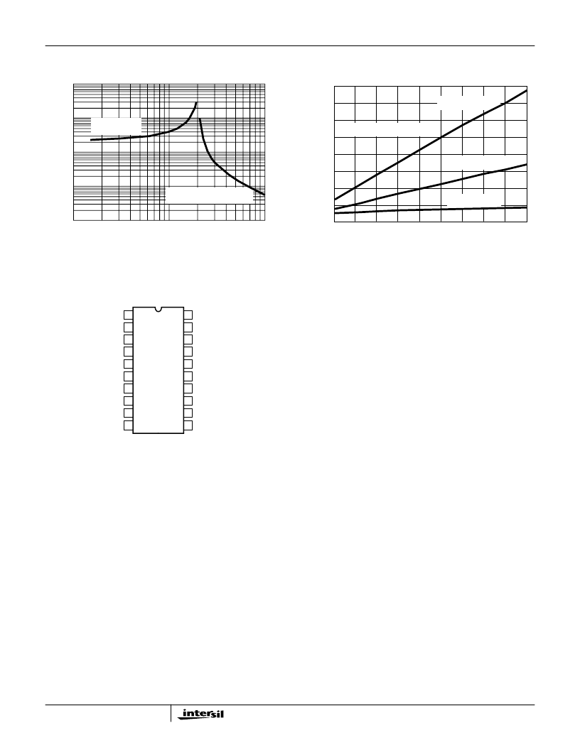
Typical Performance Curves
FIGURE 1. R
T
RESISTANCE vs FREQUENCY
FIGURE 2. BIAS SUPPLY CURRENT vs FREQUENCY
10
100
1000
SWITCHING FREQUENCY (kHz)
R
)
10
100
1000
R
T
PULLUP
TO +12V
R
T
PULLDOWN TO V
SS
100
200
300
400
500
600
700
800
900
1000
I
C
SWITCHING FREQUENCY (kHz)
C
GATE
= 3300pF
C
GATE
= 1000pF
C
GATE
= 10pF
C
UPPER
= C
LOWER
= C
GATE
80
70
60
50
40
30
20
10
0
11
12
13
14
15
16
17
18
20
19
10
9
8
7
6
5
4
3
2
1
V
SEN
OCSET
SS
VID0
VID1
VID2
VID4
VID3
COMP
FB
RT
VCC
LGATE
PGND
OVP
BOOT
UGATE
PHASE
PGOOD
GND
I
PEAK
I
-------------------------------------------
R
DS ON
)
=
HIP6014
相關(guān)PDF資料 |
PDF描述 |
|---|---|
| HIP6014CB | Buck and Synchronous-Rectifier (PWM) Controller and Output Voltage Monitor |
| HIP6016 | FPGA - 100000 SYSTEM GATE 2.5 VOLT - NOT RECOMMENDED for NEW DESIGN |
| HIP6016CB | Advanced PWM and Dual Linear Power Control |
| HIP6017B | FPGA - 100000 SYSTEM GATE 2.5 VOLT - NOT RECOMMENDED for NEW DESIGN |
| HIP6017BCB | FPGA - 100000 SYSTEM GATE 2.5 VOLT - NOT RECOMMENDED for NEW DESIGN |
相關(guān)代理商/技術(shù)參數(shù) |
參數(shù)描述 |
|---|---|
| HIP6014CB | 制造商:Rochester Electronics LLC 功能描述:- Bulk |
| HIP6014CB WAF | 制造商:Harris Corporation 功能描述: |
| HIP6014CB-T | 制造商:Rochester Electronics LLC 功能描述:- Bulk |
| HIP6015 | 制造商:INTERSIL 制造商全稱:Intersil Corporation 功能描述:Buck Pulse-Width Modulator (PWM) Controller and Output Voltage Monitor |
| HIP6015 WAF | 制造商:Harris Corporation 功能描述: |
發(fā)布緊急采購,3分鐘左右您將得到回復(fù)。