- 您現(xiàn)在的位置:買賣IC網(wǎng) > PDF目錄385381 > HIP5015EVAL2 (Intersil Corporation) () PDF資料下載
參數(shù)資料
| 型號: | HIP5015EVAL2 |
| 廠商: | Intersil Corporation |
| 英文描述: | () |
| 中文描述: | () |
| 文件頁數(shù): | 1/6頁 |
| 文件大小: | 97K |
| 代理商: | HIP5015EVAL2 |
4-108
AN9625.1
Copyright
Intersil Corporation 1996
Pentium is a registered trademark of Intel Corporation.
A Flexible DC-DC Converter for Powering High-
Performance Microprocessors (HIP5015EVAL2)
Introduction
Some of the newer, high-performance microprocessors are
migrating to a split voltage bus architecture - the processor
core is powered from a different voltage bus level than the
cache and I/O. Intel’s P55C is an upgrade Pentium
processor which employs this split bus architecture. This has
fueled a need for a power supply solution which can
seamlessly handle both power architectures. This
application note describes a Flexible DC-DC Converter
Evaluation Board (HIP5015EVAL2) that fulfills this need.
HIP5015EVAL2 Features
Meets Intel Flexible Motherboard Guidelines
Two High-Efficiency, 400kHz DC-DC Converters
Select Bit for Independent or Parallel Operation
Improved Efficiency and Reliability over Linear
Regulators
Cost Competitive with Linear Regulator Solutions
7A Total Load Current Capability, 5A Maximum per
Output
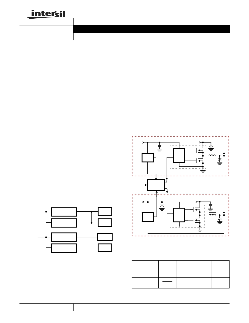
Functional Description
Figure 1 is a simple block diagram showing how two DC-DC
converters can be configured to handle either single or dual
supply microprocessor systems. The main complications to
this approach is that one converter must have a
programmable output voltage (two set points) and the two
converters must share a common load in the single supply
system.
The Flexible DC-DC Converter uses a simple technique to
address both the single and dual supply architectures.
Figure 2 is a block diagram of the Flexible DC-DC Converter;
the complete schematic and Bill of Materials of the
HIP5015EVAL2 board is included in the appendix. The
evaluation board contains two voltage-programmed DC-DC
converters, termed Converter
#
1 and Converter
#
2, and a
block of circuitry referred to as ‘gating logic’. The gating logic
has three inputs (V
SELECT
, PWM1, PWM2) and two outputs
(DR1, DR2), and programs the Flexible DC-DC Converter’s
operational mode based upon the state of V
SELECT
.
V
SELECT
is ‘programmed’ via a jumper (JP1) in the
evaluation board. Table 1 details how DR2 and V
OUT
2 are
affected by the state of V
SELECT.
DR1 and V
OUT
1 are not
altered by V
SELECT
, but PWM1 is fed through the gating
logic (and inverted) to minimize timing errors between DR1
and DR2 for accurate current-sharing in the single-supply
configuration.
FIGURE 1. BLOCK DIAGRAM OF TWO-CONVERTER
APPROACH TO SINGLE AND DUAL-SUPPLY
MICROPROCESSOR ARCHITECTURES
CORE
I/O
I/O
3.5V
3.5V
2.5V
CACHE
CORE
5V
5V
SINGLE
SUPPLY
SYSTEM
DUAL
SUPPLY
SYSTEM
3.5V
CACHE
μ
P
μ
P
DC-DC
CONVERTER #2
DC-DC
CONVERTER #1
DC-DC
CONVERTER #2
DC-DC
CONVERTER #1
TABLE 1. OUTPUT VOLTAGE PROGRAMMING BY V
SELECT
(JP1)
V
SELECT
DR1
DR2
V
OUT
1
V
OUT
2
Logic ‘1’
(JP1 open)
PWM1
PWM1
3.5V
3.5V
Logic ‘0’
(JP1 closed)
PWM1
PWM2
3.5V
2.5V
PWM1
DRIVE
PWM
+12VB
+5V
IN
V
OUT
1
PWM2
DRIVE
PWM
+12VB
+5V
IN
V
OUT
2
GATING
LOGIC
V
SELECT
DR2
HIP5015 SYNCHROFET
HIP5016 SYNCHROFET
CONVERTER #1
DR1
FIGURE 2. BLOCK DIAGRAM OF FLEXIBLE DC-DC
CONVERTER
CONVERTER #2
Application Note
August 1996
Author: Greg J. Miller
相關(guān)PDF資料 |
PDF描述 |
|---|---|
| HIP5060DW | Power Control IC Single Chip PowerSupply |
| HIP5060DY | FPGA 1000000 SYSTEM GATE 1.8 VOLT - NOT RECOMMENDED for NEW DESIGN |
| HIP6003 | Buck Pulse-Width Modulator (PWM) Controller and Output Voltage Monitor |
| HIP6003CB | Buck Pulse-Width Modulator (PWM) Controller and Output Voltage Monitor |
| HIP6004BCB | Buck and Synchronous-Rectifier (PWM) Controller and Output Voltage Monitor |
相關(guān)代理商/技術(shù)參數(shù) |
參數(shù)描述 |
|---|---|
| HIP5015IS | 制造商:Rochester Electronics LLC 功能描述:- Bulk |
| HIP5015IS WAF | 制造商:Harris Corporation 功能描述: |
| HIP5015IS1 | 制造商:Rochester Electronics LLC 功能描述:- Bulk |
| HIP5016 | 制造商:INTERSIL 制造商全稱:Intersil Corporation 功能描述:7V, 7A SynchroFET⑩ Complementary Drive Synchronous Half-Bridge |
| HIP5016IS | 制造商:Rochester Electronics LLC 功能描述:- Bulk |
發(fā)布緊急采購,3分鐘左右您將得到回復(fù)。