- 您現(xiàn)在的位置:買賣IC網(wǎng) > PDF目錄371820 > HIP1011DCA (INTERSIL CORP) XRJAX CABLE XRJAN/XRJAX - 6FT PDF資料下載
參數(shù)資料
| 型號: | HIP1011DCA |
| 廠商: | INTERSIL CORP |
| 元件分類: | 模擬信號調(diào)理 |
| 英文描述: | XRJAX CABLE XRJAN/XRJAX - 6FT |
| 中文描述: | SPECIALTY ANALOG CIRCUIT, PDSO28 |
| 封裝: | 0.150 INCH, PLASTIC, SSOP-28 |
| 文件頁數(shù): | 5/15頁 |
| 文件大小: | 139K |
| 代理商: | HIP1011DCA |
5
Absolute Maximum Ratings
Thermal Information
12VIN. . . . . . . . . . . . . . . . . . . . . . . . . . . . . . . . . . . . -0.5V to +14.0V
12VO, 12VG, 3V5VG . . . . . . . . . . . . . . . . . . . .-0.5V to 12VIN +0.5V
M12VIN . . . . . . . . . . . . . . . . . . . . . . . . . . . . . . . . . . -14.0V to +0.5V
M12VO, M12VG. . . . . . . . . . . . . . . . . . . . . . V
M12VIN
-0.5V to +0.5V
3VISEN, 5VISEN . . . . . . . . . .-0.5V to the Lesser of 12VIN or +7.0V
Voltage, Any Other Pin. . . . . . . . . . . . . . . . . . . . . . . . -0.5V to +7.0V
12VO Output Current. . . . . . . . . . . . . . . . . . . . . . . . . . . . . . . . . . .3A
M12VO Output Current . . . . . . . . . . . . . . . . . . . . . . . . . . . . . . . 0.8A
ESD Classification . . . . . . . . . . . . . . . . . . . . . . . . . . . . .2KeV (HBM)
Operating Conditions
12VIN Supply Voltage Range . . . . . . . . . . . . . . . .+10.8V to +13.2V
5V and 3.3V Input Supply Tolerances
. . . . . . . . . . . . . . . . . . . . . . ±
10%
12VO Output Current. . . . . . . . . . . . . . . . . . . . . . . . . . . . 0 to +0.5A
M12VO Output Current . . . . . . . . . . . . . . . . . . . . . . . . . . 0 to +0.1A
Temperature Range (T
A
) . . . . . . . . . . . . . . . . . . . . . . . .0
o
C to 70
o
C
Thermal Resistance (Typical, Note 1)
SSOP Package . . . . . . . . . . . . . . . . . . . . . . . . . . . .
Maximum Junction Temperature . . . . . . . . . . . . . . . . . . . . . . .150
o
C
Maximum Storage Temperature Range. . . . . . . . . . -65
o
C to 150
o
C
Maximum Lead Temperature (Soldering 10s) . . . . . . . . . . . . .300
o
C
(SSOP - Lead Tips Only)
θ
JA
(
o
C/W)
95
CAUTION: Stresses above those listed in “Absolute Maximum Ratings” may cause permanent damage to the device. This is a stress only rating and operation of the
device at these or any other conditions above those indicated in the operational sections of this specification is not implied.
NOTES:
1.
θ
JA
is measured with the component mounted on an evaluation PC board in free air.
2. All voltages are relative to GND, unless otherwise specified.
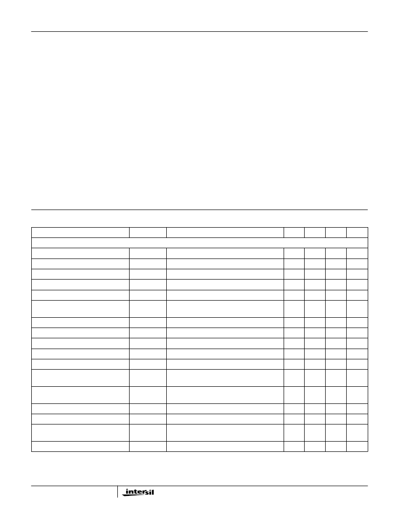
Electrical Specifications
Nominal 5.0V and 3.3V Input Supply Voltages,
12VIN = 12V, M12VIN = -12V, T
A
= T
J
= 0 to 70
o
C, Unless Otherwise Specified
PARAMETER
SYMBOL
TEST CONDITIONS
MIN
TYP
MAX
UNITS
5V/3.3V SUPPLY CONTROL
5V Overcurrent Threshold
I
OC5V
See Figure 24, Typical Application
-
8
-
A
5V Overcurrent Threshold Voltage
V
OC5V_1
V
OCSET
= 0.6V
33
42
50
mV
5V Overcurrent Threshold Voltage
V
OC5V_2
V
OCSET
= 1.2V
70
80
90
mV
5V Undervoltage Trip Threshold
V
5VUV
4.42
4.65
4.7
V
5V Undervoltage Fault Response Time
t
5VUV
-
110
160
ns
5V Turn-On Time
(PWRON High to 5VOUT = 4.75V)
t
ON5V
C
3V5VG
= 0.022
μ
F, C
5VOUT
= 2000
μ
F, R
L
= 1
-
6.5
-
ms
3V Overcurrent Threshold
I
OC3V
See Figure 24, Typical Application
-
10
-
A
3V Overcurrent Threshold Voltage
V
OC3V_1
V
OCSET
= 0.6V
41
52
62
mV
3V Overcurrent Threshold Voltage
V
OC3V_2
V
OCSET
= 1.2V
89
98
108
mV
3V Undervoltage Trip Threshold
V
3VUV
2.74
2.86
2.9
V
3V Undervoltage Fault Response Time
t
3VUV
-
110
160
ns
3V5VG Undervoltage Enable Threshold
Voltage
V
3V5VGenVth
-
9.6
-
V
3V Turn-On Time
(PWRON High to 3VOUT = 3.00V)
t
ON3V
C
3V5VG
= 0.022
μ
F, C
3VOUT
= 2000
μ
F,
R
L
= 0.43
-
6.5
-
ms
3V5VG Vout High
Vout_hi_35VG PWRON = High, FLTN = High
11.5
11.8
-
V
Gate Output Charge Current
IC
3V5VG
PWRON = High, V
3V+5VG
= 4V
19
25.0
29
μ
A
Gate Turn-On Time
(PWRON High to 3V5VG = 11V)
t
ON3V5V
C
3V5VG
= 0.033
μ
F, 3V5VG Rising 10% to 90%
-
280
-
μ
s
Gate Turn-Off Time
t
OFF3V5V
C
3V5VG
= 0.033
μ
F, 3V5VG Falling 90% to 10%
-
2
-
μ
s
HIP1011D
相關(guān)PDF資料 |
PDF描述 |
|---|---|
| HIP1011DCA-T | Dual PCI Hot Plug Controller |
| HIP1011E | Dual Slot PCI Hot Plug Controller |
| HIP1011 | PCI Hot Plug Controller |
| HIP1011CB | PCI Hot Plug Controller |
| HIP1011CB-T | PCI Hot Plug Controller |
相關(guān)代理商/技術(shù)參數(shù) |
參數(shù)描述 |
|---|---|
| HIP1011DCA-T | 功能描述:IC CTRLR HOTPLUG PCI DUAL 28SSOP RoHS:否 類別:集成電路 (IC) >> PMIC - 熱交換 系列:- 產(chǎn)品培訓(xùn)模塊:Obsolescence Mitigation Program 標(biāo)準(zhǔn)包裝:100 系列:- 類型:熱插拔開關(guān) 應(yīng)用:通用 內(nèi)部開關(guān):是 電流限制:可調(diào) 電源電壓:9 V ~ 13.2 V 工作溫度:-40°C ~ 150°C 安裝類型:表面貼裝 封裝/外殼:10-WFDFN 裸露焊盤 供應(yīng)商設(shè)備封裝:10-TDFN-EP(3x3) 包裝:管件 |
| HIP1011DCAZA | 功能描述:熱插拔功率分布 W/ANNEAL DL VER OF HIP1011 2 8LD SSOP RoHS:否 制造商:Texas Instruments 產(chǎn)品:Controllers & Switches 電流限制: 電源電壓-最大:7 V 電源電壓-最小:- 0.3 V 工作溫度范圍: 功率耗散: 安裝風(fēng)格:SMD/SMT 封裝 / 箱體:MSOP-8 封裝:Tube |
| HIP1011DCAZA-T | 功能描述:熱插拔功率分布 W/ANNEAL DL PCI HOT PLUG PWR CNTRLR RoHS:否 制造商:Texas Instruments 產(chǎn)品:Controllers & Switches 電流限制: 電源電壓-最大:7 V 電源電壓-最小:- 0.3 V 工作溫度范圍: 功率耗散: 安裝風(fēng)格:SMD/SMT 封裝 / 箱體:MSOP-8 封裝:Tube |
| HIP1011DEVAL1 | 功能描述:電源管理IC開發(fā)工具 DL SLOT PCI HOT PLUG EVALUATION BRD RoHS:否 制造商:Maxim Integrated 產(chǎn)品:Evaluation Kits 類型:Battery Management 工具用于評估:MAX17710GB 輸入電壓: 輸出電壓:1.8 V |
| HIP1011E | 制造商:未知廠家 制造商全稱:未知廠家 功能描述:Dual Slot PCI Hot Plug Controller |
發(fā)布緊急采購,3分鐘左右您將得到回復(fù)。