- 您現(xiàn)在的位置:買賣IC網(wǎng) > PDF目錄384419 > HI5810KIB (INTERSIL CORP) CMOS 10 Microsecond, 12-Bit, Sampling A/D Converter with Internal Track and Hold PDF資料下載
參數(shù)資料
| 型號: | HI5810KIB |
| 廠商: | INTERSIL CORP |
| 元件分類: | ADC |
| 英文描述: | CMOS 10 Microsecond, 12-Bit, Sampling A/D Converter with Internal Track and Hold |
| 中文描述: | 1-CH 12-BIT SUCCESSIVE APPROXIMATION ADC, PARALLEL ACCESS, PDSO24 |
| 封裝: | SOIC-24 |
| 文件頁數(shù): | 3/12頁 |
| 文件大小: | 423K |
| 代理商: | HI5810KIB |
6-1779
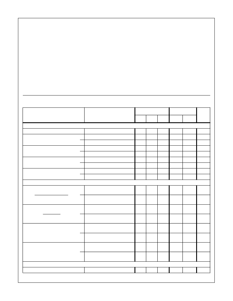
Absolute Maximum Ratings
Thermal Information
Supply Voltage
V
DD
to V
SS
. . . . . . . . . . . . . . . . . . . .(V
SS
-0.5V) < V
DD
< +6.5V
V
AA
+ to V
AA
-. . . . . . . . . . . . . . . . . . . .(V
SS
-0.5V) to (V
SS
+6.5V)
V
AA
+ to V
DD
. . . . . . . . . . . . . . . . . . . . . . . . . . . . . . . . . . . .
±
0.3V
Analog and Reference Inputs
V
IN,
V
REF
+
,
V
REF
-. . . . . . . . . (V
SS
-0.3V) < V
INA
< (V
DD
+0.3V)
Digital I/O Pins . . . . . . . . . . . . . . (V
SS
-0.3V) < VI/O < (V
DD
+0.3V)
Operating Conditions
Temperature Range
PDIP, SOIC, and CERDIP Packages . . . . . . . . . . . -40
o
C to 85
o
C
Thermal Resistance (Typical, Note 1)
CERDIP Package . . . . . . . . . . . . . . . .
PDIP Package . . . . . . . . . . . . . . . . . . .
SOIC Package. . . . . . . . . . . . . . . . . . .
Maximum Junction Temperature
Plastic Packages . . . . . . . . . . . . . . . . . . . . . . . . . . . . . . . . . 150
o
C
Hermetic Package . . . . . . . . . . . . . . . . . . . . . . . . . . . . . . . . 175
o
C
Maximum Storage Temperature Range . . . . . . . . . .-65
o
C to 150
o
C
Maximum Lead Temperature (Soldering, 10s) . . . . . . . . . . . . 300
o
C
(SOIC - Lead Tips Only)
θ
JA
(
o
C/W)
60
80
75
θ
JC
(
o
C/W)
12
N/A
N/A
CAUTION: Stresses above those listed in “Absolute Maximum Ratings” may cause permanent damage to the device. This is a stress only rating and operation
of the device at these or any other conditions above those indicated in the operational sections of this specification is not implied.
NOTE:
1.
θ
JA
is measured with the component mounted on an evaluation PC board in free air.
Electrical Specifications
V
DD
= V
AA
+ = 5V, V
REF
+ = +4.608V, V
SS
= V
AA
- = V
REF
- = GND, CLK = External 1.5MHz,
Unless Otherwise Specified
PARAMETER
TEST CONDITIONS
25
o
C
-
40
o
C TO 85
o
C
UNITS
MIN
TYP
MAX
MIN
MAX
ACCURACY
Resolution
12
-
-
12
-
Bits
Integral Linearity Error, INL
(End Point)
J
-
-
±
2.5
-
±
2.5
LSB
K
-
-
±
2.0
-
±
2.0
LSB
Differential Linearity Error, DNL
J
-
-
±
2.0
-
±
2.0
LSB
K
-
-
±
2.0
-
±
2.0
LSB
Gain Error, FSE
(Adjustable to Zero)
J
-
-
±
3.5
-
±
3.5
LSB
K
-
-
±
2.5
-
±
2.5
LSB
Offset Error, V
OS
(Adjustable to Zero)
J
-
-
±
2.5
-
±
2.5
LSB
K
-
-
±
1.5
-
±
1.5
LSB
DYNAMIC CHARACTERISTICS
Signal to Noise Ratio, SINAD
RMS Signal
RMS Noise + Distortion
J
f
S
= Internal Clock, f
IN
= 1kHz
f
S
= 1.5MHz, f
IN
= 1kHz
f
S
= Internal Clock, f
IN
= 1kHz
f
S
= 1.5MHz, f
IN
= 1kHz
f
S
= Internal Clock, f
IN
= 1kHz
f
S
= 1.5MHz, f
IN
= 1kHz
f
S
= Internal Clock, f
IN
= 1kHz
f
S
= 1.5MHz, f
IN
= 1kHz
f
S
= Internal Clock, f
IN
= 1kHz
f
S
= 1.5MHz, f
IN
= 1kHz
f
S
= Internal Clock, f
IN
= 1kHz
f
S
= 1.5MHz, f
IN
= 1kHz
f
S
= Internal Clock, f
IN
= 1kHz
f
S
= 1.5MHz, f
IN
= 1kHz
f
S
= Internal Clock, f
IN
= 1kHz
f
S
= 1.5MHz, f
IN
= 1kHz
-
68.8
62.1
-
-
-
dB
dB
K
-
71.0
63.6
-
-
-
dB
dB
Signal to Noise Ratio, SNR
RMS Signal
RMS Noise
J
-
70.5
63.2
-
-
-
dB
dB
K
-
71.5
65.0
-
-
-
dB
dB
Total Harmonic Distortion, THD
J
-
-73.9
-68.4
-
-
-
dBc
dBc
K
-
-80.3
69.7
-
-
-
dBc
dBc
Spurious Free Dynamic Range, SFDR
J
-
75.4
69.2
-
-
-
dB
dB
K
-
80.9
70.7
-
-
-
dB
dB
ANALOG INPUT
Input Current, Dynamic
At V
IN
= V
REF
+, 0V
-
±
125
±
150
-
±
150
μ
A
HI5810
相關(guān)PDF資料 |
PDF描述 |
|---|---|
| HI5810 | CMOS 10 Microsecond, 12-Bit, Sampling A/D Converter with Internal Track and Hold(CMOS 12位片內(nèi)帶跟蹤和保持電路的ADC) |
| HI5810JIB | RELAY SPDT PCB 2A 5VDC |
| HI5810JIJ | CMOS 10 Microsecond, 12-Bit, Sampling A/D Converter with Internal Track and Hold |
| HI5810JIP | CMOS 10 Microsecond, 12-Bit, Sampling A/D Converter with Internal Track and Hold |
| HI5810KIJ | CMOS 10 Microsecond, 12-Bit, Sampling A/D Converter with Internal Track and Hold |
相關(guān)代理商/技術(shù)參數(shù) |
參數(shù)描述 |
|---|---|
| HI5810KIBS2503 | 制造商:Rochester Electronics LLC 功能描述:- Bulk |
| HI5810KIJ | 制造商:Rochester Electronics LLC 功能描述:- Bulk |
| HI5810KIP | 制造商:Rochester Electronics LLC 功能描述:- Bulk |
| HI5810KIPS2503 | 制造商:Rochester Electronics LLC 功能描述:- Bulk |
| HI5812 | 制造商:INTERSIL 制造商全稱:Intersil Corporation 功能描述:CMOS 20 Microsecond, 12-Bit, Sampling A/D Converter with Internal Track and Hold |
發(fā)布緊急采購,3分鐘左右您將得到回復(fù)。