- 您現(xiàn)在的位置:買賣IC網(wǎng) > PDF目錄384408 > HI-1569PQIF (HOLT INTEGRATED CIRCUITS INC) 5V Monolithic Dual Transceiver PDF資料下載
參數(shù)資料
| 型號: | HI-1569PQIF |
| 廠商: | HOLT INTEGRATED CIRCUITS INC |
| 元件分類: | 網(wǎng)絡(luò)接口 |
| 英文描述: | 5V Monolithic Dual Transceiver |
| 中文描述: | DATACOM, MIL-STD-1553 DATA BUS TRANSCEIVER, PQFP64 |
| 封裝: | PLASTIC, ROHS COMPLIANT, QFP-64 |
| 文件頁數(shù): | 2/8頁 |
| 文件大?。?/td> | 83K |
| 代理商: | HI-1569PQIF |
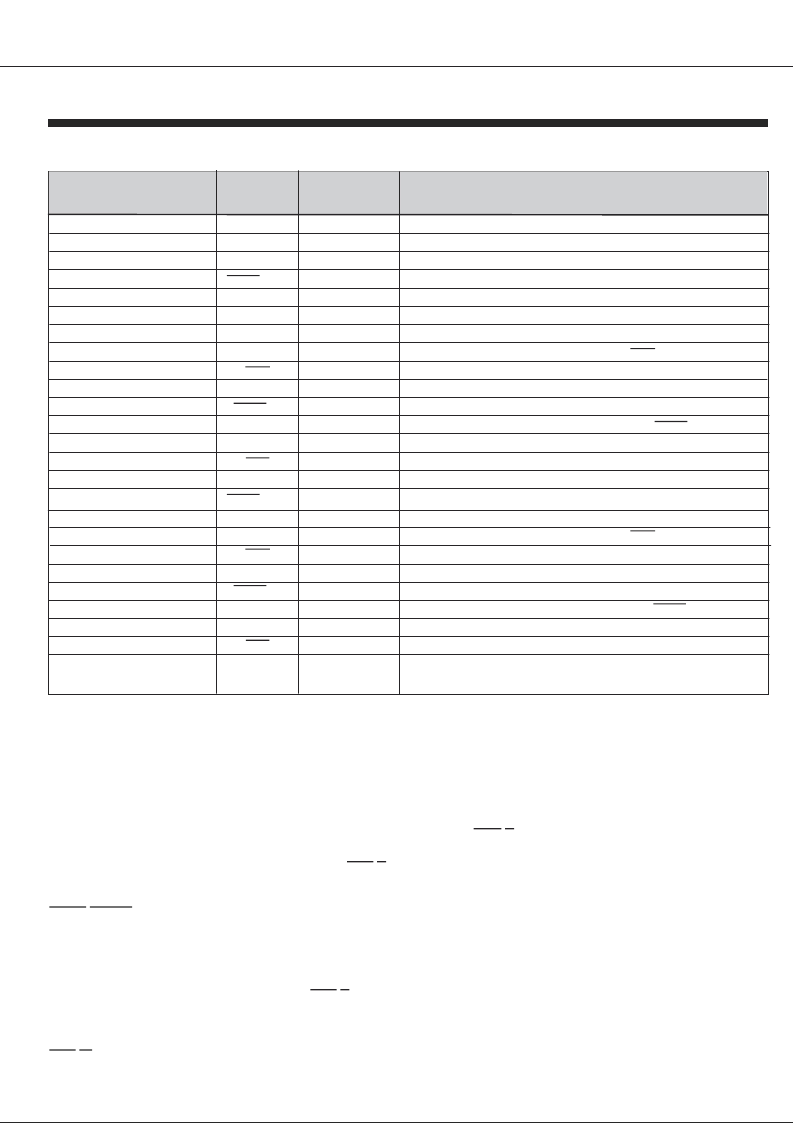
PIN DESCRIPTIONS
PIN
SYMBOL
FUNCTION
DESCRIPTION
1, 40, 50, 55
GNDA
power supply
Ground for channel A (Connect ALL pins)
2, 3
BUSA OUT
analog output
MIL-STD-1533 bus driver A, positive signal
4, 5, 44, 52, 53, 60, 61
VDDA
power supply
+5 volt power for channel A (Connect ALL pins)
6, 7
OUT
analog output
8, 18, 23, 33
GNDB
power supply
Ground for channel B (Connect ALL pins)
12, 20, 21, 28, 29, 36, 37
VDDB
14
16
25
BUSB IN
analog input
26
30
31
32
34, 35
BUSB OUT
38, 39
BUSA
MIL-STD-1533 bus driver A, negative signal
power supply
+5 volt power for channel B (Connect ALL pins)
RXB
digital output
Receiver B output, non-inverted
15
RXENB
digital input
Receiver B enable. If low, forces RXB and
low
digital output
Receiver B output, inverted
MIL-STD-1553 bus receiver B, positive signal
IN
analog input
MIL-STD-1553 bus receiver B, negative signal
TXINHB
digital input
Transmit inhibit, channel B. If high BUSB OUT,
OUT disabled
TXB
digital input
Transmitter B digital data input, non-inverted
digital input
Transmitter B digital data input, inverted
analog output
MIL-STD-1533 bus driver B, positive signal
OUT
analog output
MIL-STD-1533 bus driver B, negative signal
46
RXA
digital output
Receiver A output, non-inverted
47
RXENA
digital input
Receiver B enable. If low, forces RXB and
low
48
digital output
Receiver B output, inverted
57
BUSA IN
analog input
MIL-STD-1553 bus receiver A, positive signal
58
IN
analog input
MIL-STD-1553 bus receiver A, negative signal
62
TXINHA
digital input
Transmit inhibit, channel A. If high BUSA OUT,
OUT disabled
63
TXA
digital input
Transmitter A digital data input, non-inverted
64
digital input
Transmitter A digital data input, inverted
9 -11, 13, 17,19, 22, 24, 27
N/C
-
Not connected. May be left open or connected to power or ground
41 - 43, 45, 49, 51, 54, 56, 59
RXB
RXB
BUSB
BUSB
TXB
BUSB
RXB
RXA
BUSA
BUSA
TXA
HI-1569
HOLT INTEGRATED CIRCUITS
2
TheHI-1569databustransceivercontainsdifferentialvolt-
age source drivers and differential receivers. It is intended
for applications using a MIL-STD-1553 A/B data bus. The
device produces a trapezoidal output waveform during
transmission.
Data input to the device’s transmitter section is from the
complementary CMOS /TTL inputs TXA/B and
The transmitter accepts Manchester II bi-phase data and
converts it to differential voltages on
Thetransceiveroutputs areeitherdirector
transformer coupled to the MIL-STD-1553 data bus. Both
coupling methods produce a nominal voltage on the bus of
7.5voltspeaktopeak.
TRANSMITTER
TXA/ .
BUSA/B OUT and
/
The transmitter is automatically inhibited and placed in the
high impedance state when both TXA/B and
ther at a logic “1” or logic “0” simultaneously.Alogic “1” ap-
plied to the TXINHA/B input will force the transmitter to the
highimpedancestate,regardlessofthestateofTXA/Band
/
TXA B.
TXA/ are ei-
BUSA BOUT.
RECEIVER
The receiver accepts bi-phase differential data from the MIL-
STD-1553 bus through a direct or transformer coupled inter-
face. The receiver’s differential input stage drives a filter and
threshold comparator that produces CMOS/TTL data at the
RXA/Band
RXA/ outputpins.
Each set of receiver outputs can be independently forced to a
logic"0"bysettingRXENAorRXENBlow.
A direct coupled interface (see Figure 2) uses a 1:2.5 ratio
isolation transformer and two 55 ohm isolation resistors
betweenthetransformerandthebus.
In a transformer coupled interface (see Figure 3), the
transceiver is connected to a 1:1.79 isolation transformer
which in turn is connected to a 1:1.4 coupling transformer.The
transformer coupled method also requires two coupling
resistors equal to 75% of the bus characteristic impedence
(Zo)betweenthecouplingtransformerandthebus.
MIL-STD-1553BUSINTERFACE
FUNCTIONAL DESCRIPTION
相關(guān)PDF資料 |
PDF描述 |
|---|---|
| HI-1569PQMF | 5V Monolithic Dual Transceiver |
| HI-1569PQTF | 5V Monolithic Dual Transceiver |
| HI-1569 | 5V Monolithic Dual Transceiver |
| HI-1569PQI | 5V Monolithic Dual Transceiver |
| HI-1569PQM | 5V Monolithic Dual Transceiver |
相關(guān)代理商/技術(shù)參數(shù) |
參數(shù)描述 |
|---|---|
| HI-1569PQM | 制造商:HOLTIC 制造商全稱:Holt Integrated Circuits 功能描述:5V Monolithic Dual Transceiver |
| HI-1569PQMF | 制造商:HOLTIC 制造商全稱:Holt Integrated Circuits 功能描述:5V Monolithic Dual Transceiver |
| HI-1569PQT | 制造商:HOLTIC 制造商全稱:Holt Integrated Circuits 功能描述:5V Monolithic Dual Transceiver |
| HI-1569PQTF | 制造商:HOLTIC 制造商全稱:Holt Integrated Circuits 功能描述:5V Monolithic Dual Transceiver |
| HI-1570 | 制造商:HOLTIC 制造商全稱:Holt Integrated Circuits 功能描述:5V Monolithic Dual Variable AmplitudeTransceiver |
發(fā)布緊急采購,3分鐘左右您將得到回復(fù)。