- 您現(xiàn)在的位置:買賣IC網(wǎng) > PDF目錄296101 > HGTP3N60A4D_NL (FAIRCHILD SEMICONDUCTOR CORP) 600V, SMPS Series N-Channel IGBT with Anti-Parallel Hyperfast Diode PDF資料下載
參數(shù)資料
| 型號(hào): | HGTP3N60A4D_NL |
| 廠商: | FAIRCHILD SEMICONDUCTOR CORP |
| 元件分類: | IGBT 晶體管 |
| 英文描述: | 600V, SMPS Series N-Channel IGBT with Anti-Parallel Hyperfast Diode |
| 中文描述: | 17 A, 600 V, N-CHANNEL IGBT, TO-220AB |
| 封裝: | LEAD FREE PACKAGE-3 |
| 文件頁(yè)數(shù): | 2/9頁(yè) |
| 文件大?。?/td> | 113K |
| 代理商: | HGTP3N60A4D_NL |
2001 Fairchild Semiconductor Corporation
HGT1S3N60A4DS, HGTP3N60A4D Rev. B
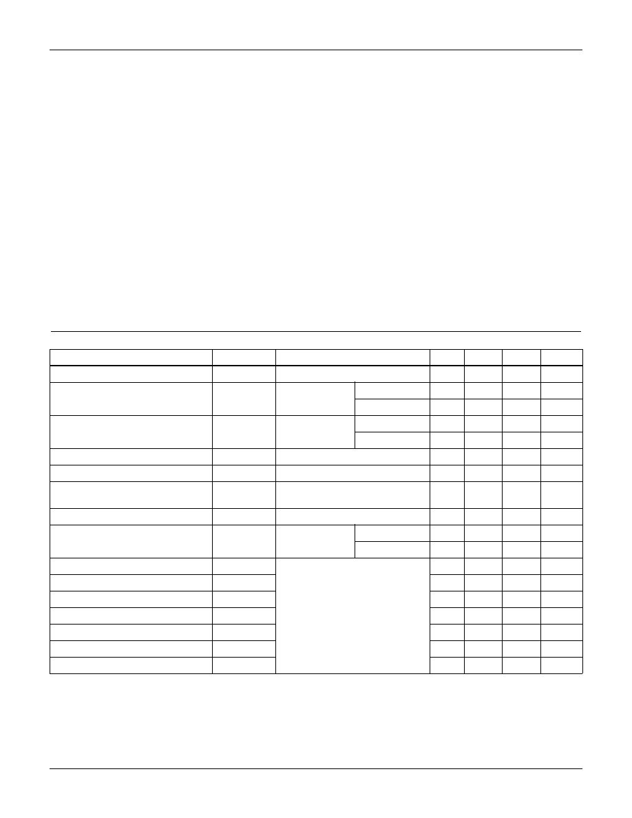
Absolute Maximum Ratings TC = 25oC, Unless Otherwise Specied
HGT1S3N60A4DS
HGTP3N60A4D
UNITS
Collector to Emitter Voltage . . . . . . . . . . . . . . . . . . . . . . . . . . . . . . . . . . . . . . . . . . . . . BVCES
600
V
Collector Current Continuous
At TC = 25
oC . . . . . . . . . . . . . . . . . . . . . . . . . . . . . . . . . . . . . . . . . . . . . . . . . . . . . . . . .I
C25
17
A
At TC = 110
oC . . . . . . . . . . . . . . . . . . . . . . . . . . . . . . . . . . . . . . . . . . . . . . . . . . . . . . .I
C110
8A
Collector Current Pulsed (Note 1) . . . . . . . . . . . . . . . . . . . . . . . . . . . . . . . . . . . . . . . . . . . ICM
40
A
Gate to Emitter Voltage Continuous . . . . . . . . . . . . . . . . . . . . . . . . . . . . . . . . . . . . . . . VGES
±20
V
Gate to Emitter Voltage Pulsed . . . . . . . . . . . . . . . . . . . . . . . . . . . . . . . . . . . . . . . . . . . VGEM
±30
V
Switching Safe Operating Area at TJ = 150
oC (Figure 2) . . . . . . . . . . . . . . . . . . . . . . . SSOA
15A at 600V
Power Dissipation Total at TC = 25
oC . . . . . . . . . . . . . . . . . . . . . . . . . . . . . . . . . . . . . . . . .P
D
70
W
Power Dissipation Derating TC > 25
oC . . . . . . . . . . . . . . . . . . . . . . . . . . . . . . . . . . . . . . . . . .
0.58
W/oC
Operating and Storage Junction Temperature Range . . . . . . . . . . . . . . . . . . . . . . . . TJ, TSTG
-55 to 150
oC
Maximum Lead Temperature for Soldering
Leads at 0.063in (1.6mm) from Case for 10s . . . . . . . . . . . . . . . . . . . . . . . . . . . . . . . . TL
Package Body for 10s, See Tech Brief 334 . . . . . . . . . . . . . . . . . . . . . . . . . . . . . . . . TPKG
300
260
oC
CAUTION: Stresses above those listed in “Absolute Maximum Ratings” may cause permanent damage to the device. This is a stress only rating and operation of the
device at these or any other conditions above those indicated in the operational sections of this specication is not implied.
NOTE:
1. Pulse width limited by maximum junction temperature.
Electrical Specications
TJ = 25
oC, Unless Otherwise Specied
PARAMETER
SYMBOL
TEST CONDITIONS
MIN
TYP
MAX
UNITS
Collector to Emitter Breakdown Voltage
BVCES
IC = 250A, VGE = 0V
600
-
V
Collector to Emitter Leakage Current
ICES
VCE = 600V
TJ = 25
oC
-
250
A
TJ = 125
oC
-
3.0
mA
Collector to Emitter Saturation Voltage
VCE(SAT)
IC = 3A,
VGE = 15V
TJ = 25
oC
-
2.0
2.7
V
TJ = 125
oC
-
1.6
2.2
V
Gate to Emitter Threshold Voltage
VGE(TH)
IC = 250A, VCE = 600V
4.5
6.1
7.0
V
Gate to Emitter Leakage Current
IGES
VGE = ±20V
-
±250
nA
Switching SOA
SSOA
TJ = 150
oC, R
G = 50, VGE = 15V,
L = 200
H, VCE = 600V
15
-
A
Gate to Emitter Plateau Voltage
VGEP
IC = 3A, VCE = 300V
-
8.8
-
V
On-State Gate Charge
Qg(ON)
IC = 3A,
VCE = 300V
VGE = 15V
-
21
25
nC
VGE = 20V
-
26
32
nC
Current Turn-On Delay Time
td(ON)I
IGBT and Diode at TJ = 25
oC,
ICE = 3A,
VCE = 390V,
VGE = 15V,
RG = 50,
L = 1mH,
Test Circuit (Figure 24)
-6
-
ns
Current Rise Time
trI
-11
-
ns
Current Turn-Off Delay Time
td(OFF)I
-73
-
ns
Current Fall Time
tfI
-47
-
ns
Turn-On Energy (Note 2)
EON1
-37
-
J
Turn-On Energy (Note 2)
EON2
-55
70
J
Turn-Off Energy (Note 3)
EOFF
-25
35
J
HGT1S3N60A4DS, HGTP3N60A4D
相關(guān)PDF資料 |
PDF描述 |
|---|---|
| HGTP7N60A4_NL | 600V SMPS Series N-Channel IGBT |
| HGXO0A-N-SM5-FREQ,10/40/-/M | CRYSTAL OSCILLATOR, CLOCK, 0.46 MHz - 50 MHz, CMOS OUTPUT |
| HGXO2F-N-50.0M,10/40/-/M | CRYSTAL OSCILLATOR, CLOCK, 50 MHz, CMOS OUTPUT |
| HGXO2G-N-32.0M,10/40/-/M | CRYSTAL OSCILLATOR, CLOCK, 32 MHz, CMOS OUTPUT |
| HGXO3A-N-460.0K,10/10/-/C | CRYSTAL OSCILLATOR, CLOCK, 0.46 MHz, CMOS OUTPUT |
相關(guān)代理商/技術(shù)參數(shù) |
參數(shù)描述 |
|---|---|
| HGTP3N60B3 | 制造商:Rochester Electronics LLC 功能描述:- Bulk 制造商:Harris Corporation 功能描述: |
| HGTP3N60B3D | 制造商:Harris Corporation 功能描述: |
| HGTP3N60B3R4724 | 制造商:Rochester Electronics LLC 功能描述:- Bulk 制造商:Harris Corporation 功能描述: |
| HGTP3N60C3 | 制造商:Rochester Electronics LLC 功能描述:- Bulk 制造商:Harris Corporation 功能描述: |
| HGTP3N60C3D | 功能描述:IGBT 晶體管 RoHS:否 制造商:Fairchild Semiconductor 配置: 集電極—發(fā)射極最大電壓 VCEO:650 V 集電極—射極飽和電壓:2.3 V 柵極/發(fā)射極最大電壓:20 V 在25 C的連續(xù)集電極電流:150 A 柵極—射極漏泄電流:400 nA 功率耗散:187 W 最大工作溫度: 封裝 / 箱體:TO-247 封裝:Tube |
發(fā)布緊急采購(gòu),3分鐘左右您將得到回復(fù)。