- 您現(xiàn)在的位置:買(mǎi)賣(mài)IC網(wǎng) > PDF目錄384386 > HB7121B (HYNIX SEMICONDUCTOR INC) CMOS IMAGE SENSOR With 8-bit ADC PDF資料下載
參數(shù)資料
| 型號(hào): | HB7121B |
| 廠商: | HYNIX SEMICONDUCTOR INC |
| 元件分類(lèi): | 模擬信號(hào)調(diào)理 |
| 英文描述: | CMOS IMAGE SENSOR With 8-bit ADC |
| 中文描述: | SPECIALTY ANALOG CIRCUIT, CQCC48 |
| 封裝: | CERAMIC, LCC-48 |
| 文件頁(yè)數(shù): | 1/29頁(yè) |
| 文件大?。?/td> | 391K |
| 代理商: | HB7121B |
當(dāng)前第1頁(yè)第2頁(yè)第3頁(yè)第4頁(yè)第5頁(yè)第6頁(yè)第7頁(yè)第8頁(yè)第9頁(yè)第10頁(yè)第11頁(yè)第12頁(yè)第13頁(yè)第14頁(yè)第15頁(yè)第16頁(yè)第17頁(yè)第18頁(yè)第19頁(yè)第20頁(yè)第21頁(yè)第22頁(yè)第23頁(yè)第24頁(yè)第25頁(yè)第26頁(yè)第27頁(yè)第28頁(yè)第29頁(yè)
HB7121B
Semiconductor Inc.
System IC SBU
DESCRIPTION
HB7121B is a highly integrated single chip CMOS B/W image sensor using Hynix 0.5um CMOS process
developed for image application to realize high efficiency photo sensor. The sensor has 414X314 pixels total,
and 400X300 pixels effective. Each pixel is high photo sensitive, small size active pixel element that converts
photons to analog voltage signal. The sensor has three on-chip 8 bit Digital to Analog Convert (DAC) and 414
comparators to digitize the pixel output. The three on-chip 8 bit DAC can be used for independent gain
control. Hynix proprietary on-chip Correlated Double Sampling (CDS) circuit can reduce Fixed Pattern Noise
(FPN) dramatically. The whole 8 bit digital B/W raw data is directly available on the package pins and just a
few control signals are needed for whole chip control, so it is very ease to configure a system using the
sensor.
FEATURES
l
400 x 300 pixels resolution
l
8um x 8um square pixel(with Microlens)
l
High efficiency photo sensors
l
Integrated 8-bit ADC for direct digital output
l
Low power 3.3V operation (5V tolerant I/O)
l
Integrated pan control and window sizing
l
Clock speed up to 15MHz
l
Programmable frame rate and synchronous format
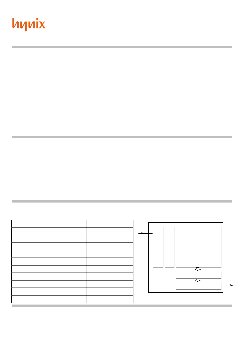
TECHNICAL SPECIFICATION FUNCTIONAL BLOCK DIAGRAM
Pixel resolution
402x302
Pixel size
8x8um
2
Fill factor(without Microlens)
30%
Format
CIF
Sensitivity
8.0V/lux
sec
Supply voltage for analog
3.3V
Supply voltage for digital
3.3V
Supply voltage for 5V tolerant input
5.0V
Power Consumption
TBD@15MHz
Operating temperature
0~40 Centigrade
Technology
0.5um 3metal CMOS
CMOS IMAGE SENSOR
With 8-bit ADC
This document is a general product description and is subject to change without notice. Hynix Semiconductor does not assume any
responsibility for use of circuits described. NO patent licenses are implied.
DA21000601R_1.1 - 1 - 2001 Hynix System IC SBU
l
Full function control through standard I
2
C bus
l
Built-in Automatic Gain Control (AGC)
l
48 pin CLCC
l
Anti-blooming circuit
l
Flexible exposure time control
l
Integrated on-chip timing and drive control
l
1/4" optical format
Pixel Array
ADC Block
Line Buffer
D
I
2
C
C
相關(guān)PDF資料 |
PDF描述 |
|---|---|
| HB7121 | CMOS IMAGE SENSOR With 8-bit ADC |
| HB7121BELECTRONICS | CMOS IMAGE SENSOR With 8-bit ADC |
| HB7131D | CMOS IMAGE SENSOR With 8-bit ADC |
| HB7141D | CMOS IMAGE SENSOR With 8-bit ADC |
| HBAT54X | Silicon Schottky Barrier Double Diodes |
相關(guān)代理商/技術(shù)參數(shù) |
參數(shù)描述 |
|---|---|
| HB7121BELECTRONICS | 制造商:HYNIX 制造商全稱(chēng):Hynix Semiconductor 功能描述:CMOS IMAGE SENSOR With 8-bit ADC |
| HB7131D | 制造商:HYNIX 制造商全稱(chēng):Hynix Semiconductor 功能描述:CMOS IMAGE SENSOR With 8-bit ADC |
| HB7141D | 制造商:HYNIX 制造商全稱(chēng):Hynix Semiconductor 功能描述:CMOS IMAGE SENSOR With 8-bit ADC |
| HB725 | 制造商:TE Connectivity 功能描述:MOD 10BASE-T - Bulk |
| HB726 | 功能描述:以太網(wǎng)模塊 HB726,MOD 10/100 RoHS:否 制造商:Lantronix 產(chǎn)品:Device Servers 數(shù)據(jù)速率:300 bps to 921.6 kbps, 10 Mbps, 100 Mbps 接口類(lèi)型:Ethernet, Serial 工作電源電壓:5 V to 15 V 工作電源電流:133 mA to 400 mA 最大工作溫度:+ 70 C |
發(fā)布緊急采購(gòu),3分鐘左右您將得到回復(fù)。