- 您現(xiàn)在的位置:買賣IC網(wǎng) > PDF目錄384385 > HA4314BCPZ (INTERSIL CORP) 400MHz, 4x1 Video Crosspoint Switch PDF資料下載
參數(shù)資料
| 型號: | HA4314BCPZ |
| 廠商: | INTERSIL CORP |
| 元件分類: | 運(yùn)動控制電子 |
| 英文描述: | 400MHz, 4x1 Video Crosspoint Switch |
| 中文描述: | 4-CHANNEL, CROSS POINT SWITCH, PDIP14 |
| 封裝: | ROHS COMPLIANT, PLASTIC, MS-001AA, DIP-14 |
| 文件頁數(shù): | 2/12頁 |
| 文件大小: | 286K |
| 代理商: | HA4314BCPZ |
2
T
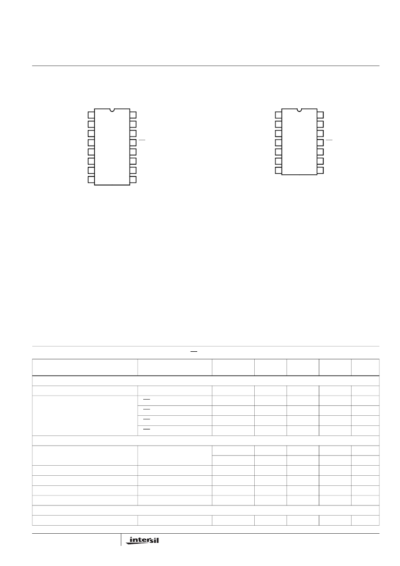
Pinouts
HA4314B
(16 LD QSOP)
TOP VIEW
HA4314B
(14 LD PDIP, SOIC)
TOP VIEW
NOTE: These pins must be left floating or connected to ground
Absolute Maximum Ratings
Thermal Information
Voltage Between V+ and V-. . . . . . . . . . . . . . . . . . . . . . . . . . . . 12V
Input Voltage . . . . . . . . . . . . . . . . . . . . . . . . . . . . . . . . . . . V
SUPPLY
Digital Input Current (Note 2). . . . . . . . . . . . . . . . . . . . . . . . .
±
25mA
Analog Input Current (Note 2) . . . . . . . . . . . . . . . . . . . . . . . . .
±
5mA
Output Current. . . . . . . . . . . . . . . . . . . . . . . . . . . . . . . . . . . . . 20mA
ESD Rating
Human Body Model (Per MIL-STD-883 Method 3015.7). . . .2000V
Operating Conditions
Temperature Range. . . . . . . . . . . . . . . . . . . . . . . . . . . 0°C to +70°C
Thermal Resistance (Typical, Note 1)
PDIP Package* . . . . . . . . . . . . . . . . . . . . . . . . . . . .
SOIC Package . . . . . . . . . . . . . . . . . . . . . . . . . . . . .
QSOP Package . . . . . . . . . . . . . . . . . . . . . . . . . . . .
Maximum Junction Temperature (Die). . . . . . . . . . . . . . . . . . +175°C
Maximum Junction Temperature (Plastic Package) . . . . . . +150°C
Maximum Storage Temperature Range. . . . . . . . . -65°C to +150°C
Maximum Lead Temperature (Soldering 10s) . . . . . . . . . . . +300°C
(SOIC and QSOP - Lead Tips Only)
*Pb-free PDIPs can be used for through hole wave solder
processing only. They are not intended for use in Reflow solder
processing applications.
θ
JA
(°C/W)
95
120
140
CAUTION: Stresses above those listed in “Absolute Maximum Ratings” may cause permanent damage to the device. This is a stress only rating and operation of the
device at these or any other conditions above those indicated in the operational sections of this specification is not implied.
NOTES:
1.
θ
JA
is measured with the component mounted on a low effective thermal conductivity test board in free air. See Tech Brief TB379 for details.
2. If an input signal is applied before the supplies are powered up, the input current must be limited to these maximum values.
15
14
13
10
1
2
3
4
5
7
6
IN0
IN1
IN2
GND
IN3
V+
A1
CS
NOTE
NOTE
A0
16
12
11
GND
GND
OUT
V-
9
8
GND
13
12
11
8
1
2
3
4
5
7
6
IN0
IN1
IN2
GND
IN3
V+
A1
CS
NC
V-
A0
14
10
9
GND
GND
OUT
Electrical Specifications
V
SUPPLY
=
±
5V, R
L
= 10k
Ω
, V
CS
= 0.8V, Unless Otherwise Specified
PARAMETER
TEST CONDITIONS
(NOTE 4)
TEMP. (°C)
MIN
TYP
MAX
UNITS
DC SUPPLY CHARACTERISTICS
Supply Voltage
Full
±
4.5
±
5.0
±
5.5
V
Supply Current (V
OUT
= 0V)
V
CS
= 0.8V
V
CS
= 0.8V
V
CS
= 2.0V
V
CS
= 2.0V
+25, +70
-
10.5
13
mA
0
-
-
15.5
mA
+25, +70
-
400
450
μ
A
0
-
400
580
μ
A
ANALOG DC CHARACTERISTICS
Output Voltage Swing without Clipping
V
OUT
= V
IN
±
V
IO
±
20mV
+25, +70
±
2.7
±
2.8
-
V
0
±
2.4
±
2.5
-
V
Output Current
Full
15
20
-
mA
Input Bias Current
Full
-
30
50
μ
A
Output Offset Voltage
Full
-10
-
10
mV
Output Offset Voltage Drift (Note 3)
Full
-
25
50
μ
V/°C
SWITCHING CHARACTERISTICS
Turn-On Time
+25
-
160
-
ns
HA4314B
相關(guān)PDF資料 |
PDF描述 |
|---|---|
| HA4314BCB | 400MHz, 4 x 1 Video Crosspoint Switch |
| HA4314BCP | 400MHz, 4 x 1 Video Crosspoint Switch |
| HA4314BCA | 400MHz, 4 x 1 Video Crosspoint Switch |
| HA4314BCA96 | 400MHz, 4 x 1 Video Crosspoint Switch |
| HA4314BCB96 | 400MHz, 4 x 1 Video Crosspoint Switch |
相關(guān)代理商/技術(shù)參數(shù) |
參數(shù)描述 |
|---|---|
| HA4314CB96 | 制造商:未知廠家 制造商全稱:未知廠家 功能描述:Interface IC |
| HA4344 | 制造商:INTERSIL 制造商全稱:Intersil Corporation 功能描述:350MHz, 4 x 1 Video Crosspoint Switch with Synchronous Controls |
| HA4344B | 制造商:INTERSIL 制造商全稱:Intersil Corporation 功能描述:350MHz, 4x1 Video Crosspoint Switch with Synchronous Controls |
| HA4344B_06 | 制造商:INTERSIL 制造商全稱:Intersil Corporation 功能描述:350MHz, 4x1 Video Crosspoint Switch with Synchronous Controls |
| HA4344BCB | 功能描述:IC SWITCH CROSS VIDEO 4:1 16SOIC RoHS:否 類別:集成電路 (IC) >> 專用 IC 系列:- 產(chǎn)品培訓(xùn)模塊:Lead (SnPb) Finish for COTS Obsolescence Mitigation Program 標(biāo)準(zhǔn)包裝:1 系列:- 類型:調(diào)幀器 應(yīng)用:數(shù)據(jù)傳輸 安裝類型:表面貼裝 封裝/外殼:400-BBGA 供應(yīng)商設(shè)備封裝:400-PBGA(27x27) 包裝:散裝 |
發(fā)布緊急采購,3分鐘左右您將得到回復(fù)。