- 您現(xiàn)在的位置:買賣IC網(wǎng) > PDF目錄384359 > GS9009ACKB (Gennum Corporation) GENLINX -TM GS9009A Cable Driver with Four Adjustable Outputs PDF資料下載
參數(shù)資料
| 型號: | GS9009ACKB |
| 廠商: | Gennum Corporation |
| 英文描述: | GENLINX -TM GS9009A Cable Driver with Four Adjustable Outputs |
| 中文描述: | GENLINX -商標(biāo)GS9009A電纜四可調(diào)輸出驅(qū)動器 |
| 文件頁數(shù): | 1/4頁 |
| 文件大?。?/td> | 73K |
| 代理商: | GS9009ACKB |
GENNUM CORPORATION P.O. Box 489, Stn. A, Burlington, Ontario, Canada L7R 3Y3
Tel. +1 (905) 632-2996 Fax. +1 (905) 632-5946 E-mail: info@gennum.com
www.gennum.com
Revision Date: June 2004
Document No. 29782 - 1
DATA SHEET
G
N
KEY FEATURES
two output pairs, adjustable from 0 to 1100mVp-p into
75
loads
nominal 600 ps rise and fall times
accepts SMPTE and standard ECL input levels
operates from a single +5 or -5 volt supply
on-chip DC restoration for low jitter
250 mW power dissipation
interfaces with GENLINX GS9002, GS9004A,
GS9005A and GS9015A
Pb-free and Green
APPLICATIONS
SMPTE 259M Serial Digital Systems (4:2:2 & 4sc)
Other Serial Digital Video Interfaces — 360Mb/s
General purpose high speed driver applications
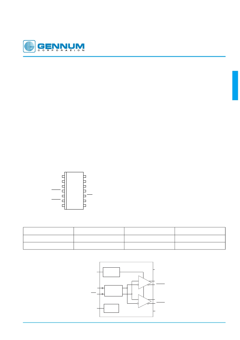
PIN CONNECTIONS
The GENLINX GS9009A is a bipolar integrated circuit
designed to drive four 75
co-axial cables at data rates
exceeding 400Mb/s. It directly interfaces with other
GENLINX devices and can also be used as a general
purpose high speed cable driver.
The differential inputs are AC-coupled and internally DC-
restored which allows correct passage of pathological
check codes associated with the serial digital standards.
Even though the inputs are AC coupled, static protection
diodes at each input restrict the DC differential so that if the
driving source uses the opposite polarity power supply,
external DC blocking capacitors must be used.
Correctly terminated output signal levels are adjustable
from as low as 0mV to as high as 1100mV with little change
in
other
performance
parameters.
guaranteed for output levels between 600 mV and 1000 mV.
The gain of the output stages is varied by adjusting the V
SET
voltage with respect to an internal bandgap reference
voltage V
REF
.
Performance
is
Pinout is compatible with the GS9007A by interchanging
pins 3,4,5,6,9,10,11,12 on the GS9009A with pins
1,2,3,4,5,6,7,8 on the GS9007A. In this way, a layout can be
made for either device depending on whether adjustability
is desired or not.
The GS9009A is packaged in a 14 pin SOIC, and operates
from a single +5 or -5 volt supply consuming typically only
250mW of power.
ORDERING INFORMATION
FUNCTIONAL BLOCK DIAGRAM
NC
NC
OUTPUT 1
OUTPUT 1
OUTPUT 2
NC
INPUT
OUTPUT 2
VSET
INPUT
VEE
VREF
NC
VCC
14
9
8
10
12
13
11
1
4
3
6
5
7
2
GS9009A
PART NUMBER
PACKAGE TYPE
TEMPERATURE RANGE
Pb-FREE AND GREEN
GS9009ACKB
14 Pin SOIC
0° to 70°C
No
GS9009ACKBE3
14 Pin SOIC
0° to 70°C
Yes
GS9009A
INPUT
V
SET
BAND-GAP
REFERENCE
INPUT BUFFER
&
DC RESTORE
V
REF
INPUT
GAIN
CONTROL
OUTPUT 1
V
CC
(GND)
OUTPUT 1
OUTPUT 2
OUTPUT 2
GND (V
EE
)
OUTPUT
DRIVER
OUTPUT
DRIVER
GENLINX
GS9009A Cable Driver
with Four Adjustable Outputs
相關(guān)PDF資料 |
PDF描述 |
|---|---|
| GS9009ACKBE3 | GENLINX -TM GS9009A Cable Driver with Four Adjustable Outputs |
| GSD2004A | Dual Common-Anode Small-Signal High-Voltage Switching Diode |
| GSD2004A-GS08 | Dual Common-Anode Small-Signal High-Voltage Switching Diode |
| GSD2004A-GS18 | Dual Common-Anode Small-Signal High-Voltage Switching Diode |
| GSD2004S | Dual In-Series Small-Signal High-Voltage Switching Diode |
相關(guān)代理商/技術(shù)參數(shù) |
參數(shù)描述 |
|---|---|
| GS9009ACKBE3 | 制造商:Semtech Corporation 功能描述:SD Cable Driver, 2 diff pairs |
| GS9009ACTBE3 | 制造商:Semtech Corporation 功能描述:TAPE & REEL 20042 in 3.9mm QSOP 16lead supplied on Reel |
| GS9009-CKB | 制造商:Gennum Corporation 功能描述: |
| GS9010 | 制造商:未知廠家 制造商全稱:未知廠家 功能描述: |
| GS9010A | 制造商:未知廠家 制造商全稱:未知廠家 功能描述:Serial Digital Automatic Tuning Subsystem |
發(fā)布緊急采購,3分鐘左右您將得到回復(fù)。