- 您現(xiàn)在的位置:買賣IC網(wǎng) > PDF目錄299162 > GS881E36BGD-200 (GSI TECHNOLOGY) 512K x 18, 256K x 32, 256K x 36 9Mb Sync Burst SRAMs PDF資料下載
參數(shù)資料
| 型號: | GS881E36BGD-200 |
| 廠商: | GSI TECHNOLOGY |
| 元件分類: | SRAM |
| 英文描述: | 512K x 18, 256K x 32, 256K x 36 9Mb Sync Burst SRAMs |
| 中文描述: | 256K X 36 CACHE SRAM, 6.5 ns, PBGA165 |
| 封裝: | 13 X 15 MM, 1 MM PITCH, ROHS COMPLIANT, FPBGA-165 |
| 文件頁數(shù): | 6/39頁 |
| 文件大小: | 815K |
| 代理商: | GS881E36BGD-200 |
第1頁第2頁第3頁第4頁第5頁當(dāng)前第6頁第7頁第8頁第9頁第10頁第11頁第12頁第13頁第14頁第15頁第16頁第17頁第18頁第19頁第20頁第21頁第22頁第23頁第24頁第25頁第26頁第27頁第28頁第29頁第30頁第31頁第32頁第33頁第34頁第35頁第36頁第37頁第38頁第39頁
GS881E18B(T/D)/GS881E32B(T/D)/GS881E36B(T/D)
Rev: 1.04a 3/2009
14/39
2002, GSI Technology
Specifications cited are subject to change without notice. For latest documentation see http://www.gsitechnology.com.
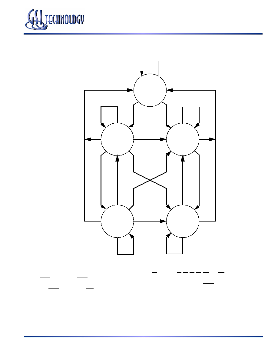
Simplified State Diagram
First Write
First Read
Burst Write
Burst Read
Deselect
R
W
CR
CW
X
WR
R
WR
X
Simple
Syn
chronous
Operation
Simple
Burst
Synchronous
Operation
CR
R
CW
CR
Notes:
1. The diagram shows only supported (tested) synchronous state transitions. The diagram presumes G is tied low.
2. The upper portion of the diagram assumes active use of only the Enable (E1) and Write (BA, BB, BC, BD, BW, and GW) control inputs, and
that ADSP is tied high and ADSC is tied low.
3. The upper and lower portions of the diagram together assume active use of only the Enable, Write, and ADSC control inputs, and
assumes ADSP is tied high and ADV is tied low.
相關(guān)PDF資料 |
PDF描述 |
|---|---|
| GS881E36BGD-200I | 512K x 18, 256K x 32, 256K x 36 9Mb Sync Burst SRAMs |
| GS881E36BGD-250 | 512K x 18, 256K x 32, 256K x 36 9Mb Sync Burst SRAMs |
| GS881E36BGD-250I | 512K x 18, 256K x 32, 256K x 36 9Mb Sync Burst SRAMs |
| GS881E36BGD-300 | 512K x 18, 256K x 32, 256K x 36 9Mb Sync Burst SRAMs |
| GS881E36BGD-300I | 512K x 18, 256K x 32, 256K x 36 9Mb Sync Burst SRAMs |
相關(guān)代理商/技術(shù)參數(shù) |
參數(shù)描述 |
|---|---|
| GS881E36BGD-200I | 制造商:GSI 制造商全稱:GSI Technology 功能描述:512K x 18, 256K x 32, 256K x 36 9Mb Sync Burst SRAMs |
| GS881E36BGD-200IV | 制造商:GSI 制造商全稱:GSI Technology 功能描述:512K x 18, 256K x 32, 256K x 36 9Mb Sync Burst SRAMs |
| GS881E36BGD-200V | 制造商:GSI 制造商全稱:GSI Technology 功能描述:512K x 18, 256K x 32, 256K x 36 9Mb Sync Burst SRAMs |
| GS881E36BGD-250 | 制造商:GSI 制造商全稱:GSI Technology 功能描述:512K x 18, 256K x 32, 256K x 36 9Mb Sync Burst SRAMs |
| GS881E36BGD-250I | 制造商:GSI 制造商全稱:GSI Technology 功能描述:512K x 18, 256K x 32, 256K x 36 9Mb Sync Burst SRAMs |
發(fā)布緊急采購,3分鐘左右您將得到回復(fù)。