- 您現(xiàn)在的位置:買賣IC網(wǎng) > PDF目錄223866 > GS8662T06BD-350I (GSI TECHNOLOGY) 8M X 8 DDR SRAM, 0.45 ns, PBGA165 PDF資料下載
參數(shù)資料
| 型號: | GS8662T06BD-350I |
| 廠商: | GSI TECHNOLOGY |
| 元件分類: | SRAM |
| 英文描述: | 8M X 8 DDR SRAM, 0.45 ns, PBGA165 |
| 封裝: | 13 X 15 MM, 1 MM PITCH, FPBGA-165 |
| 文件頁數(shù): | 2/33頁 |
| 文件大?。?/td> | 651K |
| 代理商: | GS8662T06BD-350I |
第1頁當前第2頁第3頁第4頁第5頁第6頁第7頁第8頁第9頁第10頁第11頁第12頁第13頁第14頁第15頁第16頁第17頁第18頁第19頁第20頁第21頁第22頁第23頁第24頁第25頁第26頁第27頁第28頁第29頁第30頁第31頁第32頁第33頁
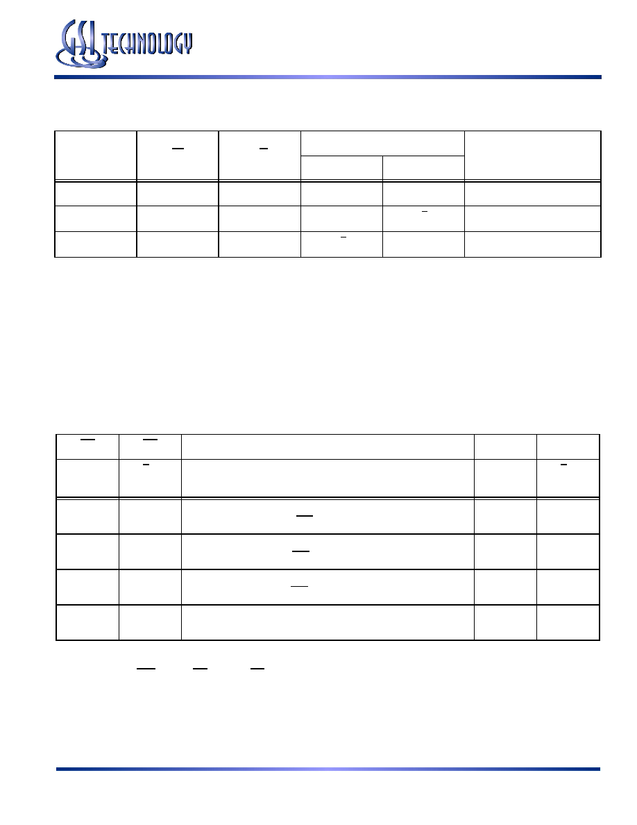
Common I/O SigmaDDR-II+ B2 SRAM Truth Table
Kn
LD
R/W
DQ
Operation
A + 0
A + 1
↑
1
X
Hi-Z / *
Deselect
↑
0
D@Kn+1
Write
↑
0
1
Q@Kn+2
Q@Kn+3
Read
Notes:
1. “1” = input “high”; “0” = input “l(fā)ow”; “V” = input “valid”; “X” = input “don’t care”.
2. D1 and D2 indicate the first and second pieces of Write Data transferred during Write operations.
3. Q1 and Q2 indicate the first and second pieces of Read Data transferred during Read operations.
4. When On-Die Termination is disabled (ODT = 0), DQ drivers are disabled (i.e., DQ pins are tri-stated) for one cycle in response to NOP
and Write commands, 2.5 cycles after the command is sampled.
5. When On-Die Termination is enabled (ODT = 1), DQ drivers are disabled for one cycle in response to NOP and Write commands, 2.5
cycles after the command is sampled. The state of the DQ pins during that time (denoted by “*” in the table above) is determined by the
state of the DQ input termination. See the Input Termination Impedance Control section for more information.
Burst of 2 Byte Write Clock Truth Table
BW
Current Operation
D
K
↑
(tn + 1)
K
↑
(tn + 1)
K
↑
(tn)
K
↑
(tn + 1)
K
↑
(tn + 1)
T
Write
Dx stored if BWn = 0 in both data transfers
D1
D2
T
F
Write
Dx stored if BWn = 0 in 1st data transfer only
D1
X
F
T
Write
Dx stored if BWn = 0 in 2nd data transfer only
X
D2
F
Write Abort
No Dx stored in either data transfer
X
Notes:
1. “1” = input “high”; “0” = input “l(fā)ow”; “X” = input “don’t care”; “T” = input “true”; “F” = input “false”.
2. If one or more BWn = 0, then BW = “T”, else BW = “F”.
Specifications cited are subject to change without notice. For latest documentation see http://www.gsitechnology.com.
Rev: 1.02 3/2011
10/33
2011, GSI Technology
GS8662T20/38BD-550/500/450/400/350
GS8662T06/11BD-500/450/400/350
相關PDF資料 |
PDF描述 |
|---|---|
| GS8662T06BD-350T | 8M X 8 DDR SRAM, 0.45 ns, PBGA165 |
| GS8672Q38BE-500I | 2M X 36 QDR SRAM, 0.45 ns, PBGA165 |
| GS880F32AGT-5.5IT | 256K X 32 CACHE SRAM, 5.5 ns, PQFP100 |
| GS880F32BGT-7IT | 256K X 32 CACHE SRAM, 7 ns, PQFP100 |
| GSAA07C-Q01 | SNAP ACTING/LIMIT SWITCH, SPDT, MOMENTARY, 0.1A, 50VDC, PANEL MOUNT |
相關代理商/技術參數(shù) |
參數(shù)描述 |
|---|---|
| GS8662T06BD-450 | 制造商:GSI Technology 功能描述:GS8662T06BD-450 - Trays |
| GS8662T06BD-500 | 制造商:GSI Technology 功能描述:GS8662T06BD-500 - Trays |
| GS8662T06BD-550 | 制造商:GSI Technology 功能描述:GS8662T06BD-550 - Trays |
| GS8662T07BD-450 | 制造商:GSI Technology 功能描述:165 FBGA - Bulk |
| GS8662T08BD-400 | 制造商:GSI Technology 功能描述:165 FBGA - Bulk |
發(fā)布緊急采購,3分鐘左右您將得到回復。