- 您現(xiàn)在的位置:買賣IC網(wǎng) > PDF目錄369690 > GS840 PDF資料下載
參數(shù)資料
| 型號: | GS840 |
| 文件頁數(shù): | 9/31頁 |
| 文件大小: | 717K |
| 代理商: | GS840 |
第1頁第2頁第3頁第4頁第5頁第6頁第7頁第8頁當前第9頁第10頁第11頁第12頁第13頁第14頁第15頁第16頁第17頁第18頁第19頁第20頁第21頁第22頁第23頁第24頁第25頁第26頁第27頁第28頁第29頁第30頁第31頁
Rev: 2.05 6/2000
Specifications cited are subject to change without notice. For latest documentation see http://www.gsitechnology.com
9/31
1999, Giga Semiconductor, Inc.
.
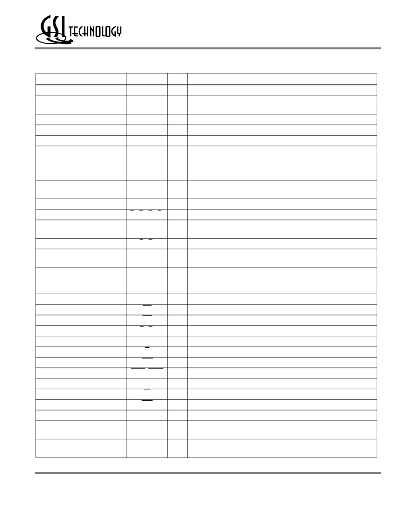
GS84018/32/36T/B-180/166/150/100
BGA Pin Description
Pin Location
N4, P4
Symbol
A
0
, A
1
Type
I
Description
Address field LSB’s and Address Counter Preset Inputs.
A2, A3, A5, A6, B3, B5, C2, C3, C5,
C6, R2, R6, T3, T5
T4
T2, T6
T2, T6
K7, K6, L7, L6, M6, N7, N6, P7
H7, H6, G7, G6, F6, E7, E6, D7
H1, H2, G1, G2, F2, E1, E2, D1
K1, K2, L1, L2, M2, N1, N2, P1
An
I
Address Inputs
An
NC
An
Address Input (x32/36 Versions)
No Connect (x32/36 Versions)
Address Input (x18 Version)
-
I
DQ
A1
-DQ
A8
DQ
B1
-DQ
B8
DQ
C1
-DQ
C8
DQ
D1
-DQ
D8
DQ
A9
, DQ
B9
,
DQ
C9
, DQ
D9
NC
B
A
, B
B
, B
C
, B
D
DQ
A1
-DQ
A9
DQ
B1
-DQ
B9
B
A
, B
B
I/O
Data Input and Output pins. (x32/36 Versions)
P6, D6, D2, P2
I/O
Data Input and Output pins. (x36 Version)
P6, D6, D2, P2
L5, G5, G3, L3
-
I
No Connect (x32 Version)
Byte Write Enable for DQ
A
, DQ
B
, DQ
C
, DQ
D
I/O’s. Active Low. ( x36 Version)
P7, N6, L6, K7, H6, G7, F6, E7, D6
D1, E2, G2, H1, K2, L1, M2, N1, P2
L5, G3
B1, C1, R1, T1, U2, J3, U3, D4, L4,
U4, J5, U5, U6, B7, C7, R7
P6, N7, M6, L7, K6, H7, G6, E6, D7,
D2, B1, E1, F2, G1, H2, K1, L2, N2,
P1, G5, L3, T4
K4
M4
H4
E4, B6
B2
F4
G4
A4, B4
T7
R5
R3
J2, C4, J4, R4, J6
D3, E3, F3, H3, K3, M3, N3, P3, D5,
E5, F5, H5, K5, M5, N5, P5
A1, F1, J1, M1, U1, A7, F7, J7, M7,
U7
I/O
Data Input and Output pins. (x18 Version)
I
Byte Write Enable for DQ
A
, DQ
B
I/O’s. Active Low. ( x18 Version)
NC
-
No Connect
NC
-
No Connect (x18 Version)
CK
BW
GW
E
1
, E
3
E
2
G
ADV
I
I
I
I
I
I
I
I
I
I
I
I
Clock Input Signal. Active High.
Byte Write. Writes all enabled bytes. Active Low.
Global Write Enable. Writes all bytes. Active Low.
Chip Enable. Active Low.
Chip Enable. Active High.
Output Enable. Active Low.
Burst address counter advance enable. Active Low.
Address Strobe (Processor, Cache Controller). Active Low.
Sleep Mode control. Active High.
Flow Through or Pipeline mode. Active Low.
Linear Burst Order mode. Active Low.
Core power supply.
ADSP, ADSC
ZZ
FT
LBO
V
DD
V
SS
I
I/O and Core Ground.
V
DDQ
I
Output driver power supply.
This Material Copyrighted by Its Respective Manufacturer
相關(guān)PDF資料 |
PDF描述 |
|---|---|
| GS84018B-100 | x18 Fast Synchronous SRAM |
| GS84018B-100I | x18 Fast Synchronous SRAM |
| GS84018B-100IT | x18 Fast Synchronous SRAM |
| GS84018B-150 | x18 Fast Synchronous SRAM |
| GS84032B-100 | x32 Fast Synchronous SRAM |
相關(guān)代理商/技術(shù)參數(shù) |
參數(shù)描述 |
|---|---|
| GS84018 | 制造商:未知廠家 制造商全稱:未知廠家 功能描述:256K x 18, 128K x 32, 128K x 36 4Mb Sync Burst SRAMs |
| GS84018/32/36T/B-180/166/150/100 | 制造商:未知廠家 制造商全稱:未知廠家 功能描述:256K x 18 128K x 32 128K x 36 4Mb Sync Burst |
| GS84018AB-100 | 制造商:GSI Technology 功能描述:SRAM SYNC SGL 3.3V 4.5MBIT 256KX18 12NS/4.5NS 119FBGA - Trays |
| GS84018AB-100I | 制造商:GSI Technology 功能描述:SRAM SYNC SGL 3.3V 4.5MBIT 256KX18 12NS/4.5NS 119FBGA - Trays |
| GS84018AB-150 | 制造商:GSI Technology 功能描述:SRAM SYNC SGL 3.3V 4.5MBIT 256KX18 10NS/3.8NS 119FBGA - Trays |
發(fā)布緊急采購,3分鐘左右您將得到回復。