- 您現(xiàn)在的位置:買賣IC網(wǎng) > PDF目錄369690 > GS84018T-100I x18 Fast Synchronous SRAM PDF資料下載
參數(shù)資料
| 型號(hào): | GS84018T-100I |
| 英文描述: | x18 Fast Synchronous SRAM |
| 中文描述: | x18快速同步SRAM |
| 文件頁數(shù): | 12/31頁 |
| 文件大?。?/td> | 717K |
| 代理商: | GS84018T-100I |
第1頁第2頁第3頁第4頁第5頁第6頁第7頁第8頁第9頁第10頁第11頁當(dāng)前第12頁第13頁第14頁第15頁第16頁第17頁第18頁第19頁第20頁第21頁第22頁第23頁第24頁第25頁第26頁第27頁第28頁第29頁第30頁第31頁
Rev: 2.05 6/2000
Specifications cited are subject to change without notice. For latest documentation see http://www.gsitechnology.com
12/31
1999, Giga Semiconductor, Inc.
.
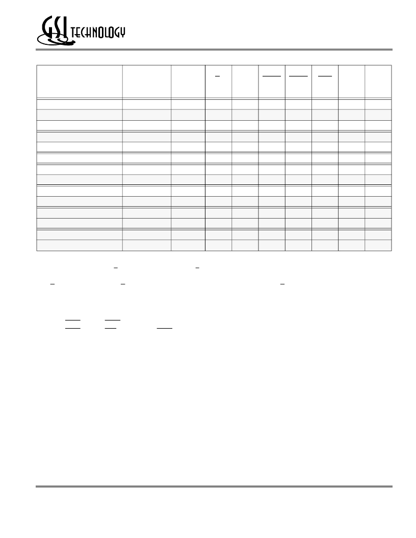
GS84018/32/36T/B-180/166/150/100
Synchronous Truth Table
Operation
Address Used
State
Diagram
Key
5
X
X
X
R
R
W
CR
CR
CW
CW
E
1
E
2
ADSP
ADSC
ADV
W
3
DQ
4
Deselect Cycle, Power Down
Deselect Cycle, Power Down
Deselect Cycle, Power Down
Read Cycle, Begin Burst
Read Cycle, Begin Burst
Write Cycle, Begin Burst
Read Cycle, Continue Burst
Read Cycle, Continue Burst
Write Cycle, Continue Burst
Write Cycle, Continue Burst
Read Cycle, Suspend Burst
Read Cycle, Suspend Burst
Write Cycle, Suspend Burst
Write Cycle, Suspend Burst
Note:
1.
X = Don’t Care, H = High, L = Low.
2.
E = T (True) if E
2
= 1 and E
3
= 0; E = F (False) if E
2
= 0 or E
3
= 1.
3.
W = T (True) and F (False) is defined in the Byte Write Truth Table preceding.
4.
G is an asynchronous input. G can be driven high at any time to disable active output drivers. G low can only enable active drivers (shown
as “Q” in the Truth Table above).
None
None
None
External
External
External
Next
Next
Next
Next
Current
Current
Current
Current
H
L
L
L
L
L
X
H
X
H
X
H
X
H
X
F
F
T
T
T
X
X
X
X
X
X
X
X
X
L
H
L
H
H
H
X
H
X
H
X
H
X
L
X
L
X
L
L
H
H
H
H
H
H
H
H
X
X
X
X
X
X
L
L
L
L
H
H
H
H
X
X
X
X
F
T
F
F
T
T
F
F
T
T
High-Z
High-Z
High-Z
Q
Q
D
Q
Q
D
D
Q
Q
D
D
5.
All input combinations shown above are tested and supported. Input combinations shown in gray boxes need not be used to accomplish
basic synchronous or synchronous burst operations and may be avoided for simplicity.
Tying ADSP high and ADSC low allows simple non-burst synchronous operations. See
BOLD
items above.
Tying ADSP high and ADV low while using ADSC to load new addresses allows simple burst operations. See
ITALIC
items above.
6.
7.
This Material Copyrighted by Its Respective Manufacturer
相關(guān)PDF資料 |
PDF描述 |
|---|---|
| GS84018T-100IT | x18 Fast Synchronous SRAM |
| GS84018T-150 | x18 Fast Synchronous SRAM |
| GS84018T-150I | x18 Fast Synchronous SRAM |
| GS84018T-150IT | x18 Fast Synchronous SRAM |
| GS84018T-166 | x18 Fast Synchronous SRAM |
相關(guān)代理商/技術(shù)參數(shù) |
參數(shù)描述 |
|---|---|
| GS84018T-100IT | 制造商:未知廠家 制造商全稱:未知廠家 功能描述:x18 Fast Synchronous SRAM |
| GS84018T-150 | 制造商:未知廠家 制造商全稱:未知廠家 功能描述:x18 Fast Synchronous SRAM |
| GS84018T-150I | 制造商:未知廠家 制造商全稱:未知廠家 功能描述:x18 Fast Synchronous SRAM |
| GS84018T-150IT | 制造商:未知廠家 制造商全稱:未知廠家 功能描述:x18 Fast Synchronous SRAM |
| GS84018T-166 | 制造商:未知廠家 制造商全稱:未知廠家 功能描述:x18 Fast Synchronous SRAM |
發(fā)布緊急采購,3分鐘左右您將得到回復(fù)。