- 您現(xiàn)在的位置:買賣IC網(wǎng) > PDF目錄383001 > GL652USB (Electronic Theatre Controls, Inc.) USB 7 PORT HUB CONTROLLER PDF資料下載
參數(shù)資料
| 型號: | GL652USB |
| 廠商: | Electronic Theatre Controls, Inc. |
| 英文描述: | USB 7 PORT HUB CONTROLLER |
| 中文描述: | 7端口的USB集線器控制器 |
| 文件頁數(shù): | 8/17頁 |
| 文件大小: | 190K |
| 代理商: | GL652USB |

8 08/18/00
GL652USB 7 PORT USB HUB CONTROLLER
Revision 1.2
After filling the data-to-transmit into FF0, the micro-controller should setup this register to
enable endpoint 0 data transmit. If EP0OE = 0, endpoint 0 will respond to a valid IN transaction
with a NAK. EP0OE will be automatically cleared after a successful transmission, or when
endpoint 0 has incidentally accepted another SETUP or OUT transaction.
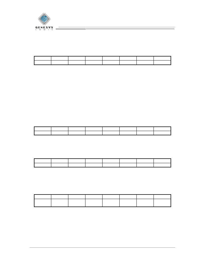
( offset 04, default = 00h )
R/W
R/W
R/W
R/O
EP1STL
EP1OE
EP1SEQ
EP1CNT3
Endpoint 1 transmit setting –
EP1CNT3~0
: number of data bytes to transmit. EP1CNT3~1 are always ‘0’.
EP1OE
: enable data transmit
1 – ready to transmit data packet
0 – not ready to transmit data packet (default)
EP1SEQ
: data packet type
0 –DATA0
1 –DATA1
EP1STL
: set endpoint 1 stall
1 – EP1 will respond to USB host controller with STALL packet
0 – default
After preparing the data to transmit, the micro-controller should setup this register to enable
endpoint 1 data transmit. If EP1OE = 0, endpoint 1 will respond to a valid IN transaction with a
NAK. After a successful transmission, the device will automatically clear EP1OE.
( offset 05, default = 00h )
R/W
R/W
R/W
R/W
FFD7
FFD6
FFD5
FFD4
If FFSEL1 (in BUFCTL) = 1’b0, this is FF0 access-window; if FFSEL1 = 1’b1, this is FF1
access-window. Each FFDAT read/write will automatically increase the FIFO pointer, which is
a 3-bit circular counter, by 1. Writing FPRST with ‘1’ (in BUFCTL) will reset the pointer. Note
that to fill FF0, RXDIS (in RXCTL0) must be first cleared.
BUFCTL
( offset 06 )
--
--
--
--
Data buffer control –
FFSEL1
: FIFO 0/1 selector
1’b0 – select endpoint 0 data buffer
1’b1 – select endpoint 1 data buffer
FPRST
: reset FIFO 0/1 pointer (write only)
PORTSEL
( offset 07, default = 00h )
R/W
R/W
R/W
--
PORTSEL
7
6
5
PORTSEL
: PORT 1~7 under request
PORTSEL1
1’b1 – port 1 selected
PORTSEL2
1’b1 – port 2 selected
PORTSEL3
1’b1 – port 3 selected
PORTSEL4
1’b1 – port 4 selected
PORTSEL5
1’b1 – port 4 selected
PORTSEL6
1’b1 – port 4 selected
PORTSEL7
1’b1 – port 4 selected
TXCTL1
R/O
R/O
R/W
--
EP1CNT2
EP1CNT1
EP1CNT0
FFDAT
R/W
FFD3
R/W
FFD2
R/W
FFD1
R/W
FFD0
W/O
FPRST
R/W
FFSEL1
--
--
R/W
R/W
R/W
R/W
PORTSEL
PORTSEL
PORTSEL
4
PORTSEL
3
PORTSEL
2
PORTSEL
1
相關(guān)PDF資料 |
PDF描述 |
|---|---|
| GL811E | USB 2.0 to ATA / ATAPI Bridge Controller |
| GL813 | USB 2.0 CompactFlash Card Reader Controller |
| GL911Tx | Wireless Mouse Transmitter Controller |
| GLT41016 | 64K X 16 CMOS DYNAMIC RAM WITH EXTENDED DATA OUTPUT |
| GLT41016-30J4 | 64K X 16 CMOS DYNAMIC RAM WITH EXTENDED DATA OUTPUT |
相關(guān)代理商/技術(shù)參數(shù) |
參數(shù)描述 |
|---|---|
| GL6551 | 制造商:HYNIX 制造商全稱:Hynix Semiconductor 功能描述:COMPANDER |
| GL6552 | 制造商:HYNIX 制造商全稱:Hynix Semiconductor 功能描述:Low Voltage Compander |
| GL65-KIT | 制造商:Sola/Hevi-Duty 功能描述:Mating Connector Kit |
| GL6718 | 制造商:GTM 制造商全稱:GTM 功能描述:NPN EPITAXIAL PLANAR TRANSISTOR |
| GL6840 | 制造商:HYNIX 制造商全稱:Hynix Semiconductor 功能描述:Electronic Two Tone Ringer |
發(fā)布緊急采購,3分鐘左右您將得到回復(fù)。