- 您現(xiàn)在的位置:買賣IC網(wǎng) > PDF目錄382995 > GB4571-CDA (Electronic Theatre Controls, Inc.) Video Buffer with Precision Strobed DC Restore PDF資料下載
參數(shù)資料
| 型號: | GB4571-CDA |
| 廠商: | Electronic Theatre Controls, Inc. |
| 英文描述: | Video Buffer with Precision Strobed DC Restore |
| 中文描述: | 視頻緩沖區(qū)精密選通DC恢復(fù) |
| 文件頁數(shù): | 1/5頁 |
| 文件大小: | 149K |
| 代理商: | GB4571-CDA |
The GB4571 is a high performance video buffer with DC
restore used primarily for accurate back porch clamping. Key
features include operation from
±
4.5 V to
±
13.2 V supply
voltages, fast recovery from sudden changes in DC offset,
±
0.1 dB flatness to 80 MHz and availability of industry standard
DIP and SOIC packages.
In the typical back porch clamping application, a negative
going back porch pulse from an external sync separator (such
as the GS4881 or GS4882) is applied to the GB4571's STROBE
input. While STROBE is low, the GB4571 determines the
correct DC level shift that should be applied to the input signal
by integrating over the entire back porch period. This reduces
sensitivity to noise and improves the accuracy of the DC
restoration compared to systems using sample and hold
techniques. Typical clamping accuracy of
±
1 mV is achieved
by the GB4571.
Clamping of NTSC, PAL, SECAM & RGB Video Signals
Multimedia Graphics Overlay
Production Switchers
Linear Keyers
Part Number
Package
Temperature Range
GB4571-CDA 8 pin PDIP
0
°
to 70
°
C
GB4571-CKA 8 pin SOIC
0
°
to 70
°
C
GB4571-CTA 8 pin SOIC Tape
0
°
to 70
°
C
DATA SHEET
GENNUM CORPORATION P.O. Box 489, Stn A, Burlington, Ontario, Canada L7R 3Y3 tel. (905) 632-2996 fax: (905) 632-2055
Japan Branch: A-302, Miyamae Village, 2-10-42, Miyamae, Suginami-ku, Tokyo 168, Japan tel. (03) 3247-8838 fax. (03) 3247-8839
GB4571 Video Buffer with
Precision Strobed DC Restore
FEATURES
DESCRIPTION
AVAILABLE PACKAGING
8 pin PDIP
8 pin SOIC
PIN CONNECTIONS
1
2
3
4
8
7
6
5
V
CC
V
OUT
V
EE
GND
C
HOLD
V
IN
V
CLAMP
STROBE
GB4571
ORDERING INFORMATION
APPLICATIONS
accurate clamping to within
±
1 mV
less than 1 mV clamping distortion
variable clamping range (V
EE
+ 3.0 V to V
CC
- 4.5 V)
ultra low differential gain and differential phase
fast recovery from sudden changes in DC offsets
less than
±
0.15
°
phase delay variation at 3.58 MHz
±
0.1 dB flatness to 80 MHz
±
4.5 V to
±
13.2 V supply voltage range
Document No. 521 - 17 - 01
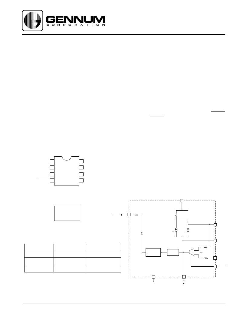
SIMPLIFIED CIRCUIT DIAGRAM
C
HOLD
GND
VCC
V
EE
V
IN
COUPLING
V
OUT
STROBE
V
CLAMP
-
+
7
3
1
5
2
HIGH Z
NON-LNEAR
V TO
I
CONVERTER
4
6
8
相關(guān)PDF資料 |
PDF描述 |
|---|---|
| GB4571-CKA | Video Buffer with Precision Strobed DC Restore |
| GBJ1501 | Single Phase Bridge Rectifiers |
| GBJ15005 | Single Phase Bridge Rectifiers |
| GBJ1502 | Single Phase Bridge Rectifiers |
| GBJ1504 | Single Phase Bridge Rectifiers |
相關(guān)代理商/技術(shù)參數(shù) |
參數(shù)描述 |
|---|---|
| GB4571CKA | 制造商:Gennum Corporation 功能描述: |
| GB4571-CKA | 制造商:未知廠家 制造商全稱:未知廠家 功能描述:Video Buffer with Precision Strobed DC Restore |
| GB4571CKAE3 | 制造商:Gennum 功能描述: 制造商:Gennum Corporation 功能描述: |
| GB4571-CKAE3 | 制造商:Semtech Corporation 功能描述: 制造商:Semtech Corporation 功能描述:Video Buffers & Clamps |
| GB4571-CTA | 制造商:GENNUM 制造商全稱:GENNUM 功能描述:Video Buffer with Precision Strobed DC Restore |
發(fā)布緊急采購,3分鐘左右您將得到回復(fù)。