- 您現(xiàn)在的位置:買賣IC網(wǎng) > PDF目錄97949 > FWLF1634RL19 FIBER OPTIC TRANSCEIVER, 1537-1587nm, 4250Mbps(Tx), 4250Mbps(Rx), SURFACE MOUNT, SFP CONNECTOR PDF資料下載
參數(shù)資料
| 型號: | FWLF1634RL19 |
| 元件分類: | 光收發(fā) |
| 英文描述: | FIBER OPTIC TRANSCEIVER, 1537-1587nm, 4250Mbps(Tx), 4250Mbps(Rx), SURFACE MOUNT, SFP CONNECTOR |
| 文件頁數(shù): | 8/11頁 |
| 文件大?。?/td> | 351K |
| 代理商: | FWLF1634RL19 |

FWLF1634RLxx DWDM SFP Product Specification – August 2010
F i n i s a r
Finisar Corporation
Page 6
Rev D1, Aug.2010
V.
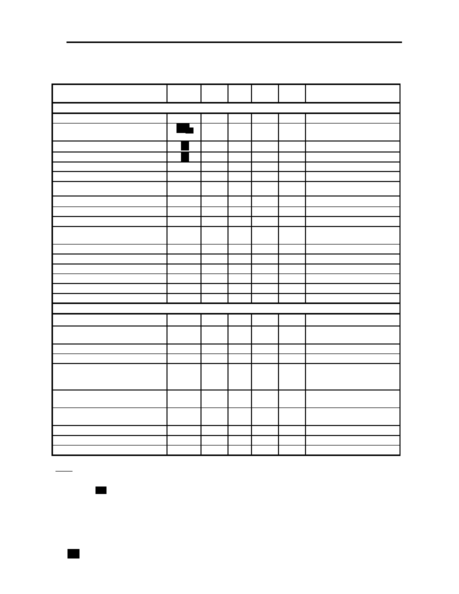
Optical Parameters
1
Parameter
Symbol
Min
Typ
Max
Units Notes/Conditions
TRANSMITTER CHARACTERISTICS
Center Wavelength Spacing
100
GHz
Corresponds to approximately 0.8 nm
Modulated Spectral Width
0.2
0.3
nm
Full width, -20dB from max.
See note 3
Center Wavelength – End of Life
c
X - 100
X
X + 100
pm
X = specified center wavelength
Center Wavelength – BOL Offset
c
Y - 25
Y
Y + 25
pm
Y = specified center wavelength
Side Mode Suppression Ratio
SMSR
30
dB
Modulated
Optical Rise/Fall Time
tr / tf
120
ps
Unfiltered, 80% -20%
Optical Output Power
Pout
+2
+5
dBm
Avg. power coupled into SMF-28; see
note 4
Extinction Ratio, (<=4.25G)
OMI
6.0
dB
EOL
Extinction Ratio, SONET
OMI
8.2
dB
EOL, Rate Select Option Only
Eye Opening
10
%
Jitter Generation, SONET
75
mUI
Parameters per GR-253
2
section 5.6 for OC-48 B
Total Jitter
59.8
ps
(p-to-p)
Deterministic Jitter
28.2
ps
(p-to-p)
Reflectance
RTX
-27
dB
Tolerable Back Reflection
BR
-14
dB
See note 5
Relative Intensity Noise
RIN
-120
dB/Hz
Dispersion Power Penalty
DPP
3.0
dB
At 1600 ps/nm. See Note 6
RECEIVER CHARACTERISTICS
Optical Input Wavelength
Pin
1520
1570
nm
Jitter Generation , SONET
75
mUI
Parameters per GR-253
2
section 5.6 for OC-48 B
Total Jitter
61.8
ps
(p-to-p)
Deterministic Jitter
25.9
ps
(p-to-p)
Optical Input Power
(BER < 10
-12)
Pin
-28
-9
dBm
2.5 Gb/s w/ PRBS 2
23 -1
EOL, & rate select low option
implemented
Optical Input Power
(BER < 10
-12)
Pin
-23
-9
dBm
4.25 Gb/s w/ PRBS 2
7 -1
EOL
Optical Input Power –
Receiver Damage Threshold
+6
dBm
Receiver Reflectance
RRX
-27
dB
Min-Required OSNR 0ps/nm
OSNRbb
22
dB
See Note 7
Min-Required OSNR 1600ps/nm
OSNRt
25
dB
See Note 7
Notes:
1. Parameters are specified over temperature and voltage, at end of life, and for non-rate select option unless otherwise noted.
2. All parameters are measured on a Finisar SFP Evaluation Card unless otherwise noted.
3. For accurate
20 measurements, an OSA with a resolution band width of ≤ 20pm is recommended.
4. Output power of +3 to +7dBm is also supported; please contact your local Finisar sales representatives for details.
5. Tolerable back reflection is the max back reflection level at which the power penalty will be <1dB. Power penalty is measured
over fiber (1600ps/nm) at BER = 10
-12 with OSNR set at 24dB.
6. Dispersion power penalty is measured in loop back with OSNR set to 30 dB. Data rate and pattern used same as specified for
Optical Input Power. Dispersion power penalty is the difference in Rx power at a BER of 10
-12 for 0ps/nm & 1600ps/nm
7. Rx power set between -9dBm and -18dBm. Data rate and pattern used same as specified for Optical Input Power. Measured as
the Minimum OSNR to achieve a BER of 10
-12 . Optical filter bandwidth of 0.1nm is used in OSNR measurement.
相關(guān)PDF資料 |
PDF描述 |
|---|---|
| FWLF1634RL20 | FIBER OPTIC TRANSCEIVER, 1536-1586nm, 4250Mbps(Tx), 4250Mbps(Rx), SURFACE MOUNT, SFP CONNECTOR |
| FWLF1634RL22 | FIBER OPTIC TRANSCEIVER, 1535-1585nm, 4250Mbps(Tx), 4250Mbps(Rx), SURFACE MOUNT, SFP CONNECTOR |
| FWLF1634RL24 | FIBER OPTIC TRANSCEIVER, 1533-1583nm, 4250Mbps(Tx), 4250Mbps(Rx), SURFACE MOUNT, SFP CONNECTOR |
| FWLF1634RL25 | FIBER OPTIC TRANSCEIVER, 1532-1582nm, 4250Mbps(Tx), 4250Mbps(Rx), SURFACE MOUNT, SFP CONNECTOR |
| FWLF1634RL27 | FIBER OPTIC TRANSCEIVER, 1531-1581nm, 4250Mbps(Tx), 4250Mbps(Rx), SURFACE MOUNT, SFP CONNECTOR |
相關(guān)代理商/技術(shù)參數(shù) |
參數(shù)描述 |
|---|---|
| FWLF1634RL20 | 制造商:Finisar Corporation 功能描述:TXRX DWDM 4GBPS APD SFP |
| FWLF1634RL21 | 制造商:Finisar Corporation 功能描述:TXRX DWDM 4GBPS APD SFP |
| FWLF1634RL22 | 制造商:Finisar Corporation 功能描述:TXRX DWDM 4GBPS APD SFP |
| FWLF1634RL23 | 制造商:Finisar Corporation 功能描述:TXRX DWDM 4GBPS APD SFP |
| FWLF1634RL24 | 制造商:Finisar Corporation 功能描述:TXRX DWDM 4GBPS APD SFP |
發(fā)布緊急采購,3分鐘左右您將得到回復(fù)。