- 您現(xiàn)在的位置:買賣IC網(wǎng) > PDF目錄375865 > FOD250L (FAIRCHILD SEMICONDUCTOR CORP) HIGH SPEED TRANSISTOR OPTOCOUPLERS PDF資料下載
參數(shù)資料
| 型號: | FOD250L |
| 廠商: | FAIRCHILD SEMICONDUCTOR CORP |
| 元件分類: | 光電耦合器 |
| 英文描述: | HIGH SPEED TRANSISTOR OPTOCOUPLERS |
| 中文描述: | 1 CHANNEL LOGIC OUTPUT OPTOCOUPLER |
| 封裝: | DIP-8 |
| 文件頁數(shù): | 4/13頁 |
| 文件大?。?/td> | 689K |
| 代理商: | FOD250L |
6/14/04
Page 4 of 13
2004 Fairchild Semiconductor Corporation
LVTTL/LVCMOS 3.3V
HIGH SPEED TRANSISTOR
OPTOCOUPLERS
SINGLE-CHANNEL: FOD050L
DUAL-CHANNEL:
FOD250L
FOD053L
** All Typicals at T
A
= 25°C
Notes
1.
2.
3. The 4.1 k
4.
Common mode transient immunity in logic high level is the maximum tolerable (positive) dV
common mode pulse signal V
CM
, to assure that the output will remain in a logic high state (i.e., V
transient immunity in logic low level is the maximum tolerable (negative) dV
pulse signal, V
CM
, to assure that the output will remain in a logic low state (i.e., V
5. Device is considered a two terminal device: Pins 1, 2, 3 and 4 are shorted together and Pins 5, 6, 7 and 8 are shorted
together.
Current Transfer Ratio is defined as a ratio of output collector current, I
The 1.9 k
load represents 1 TTL unit load of 1.6 mA and 5.6 k
load represents 1 LSTTL unit load of 0.36 mA and 6.1k
O
, to the forward LED input current, I
pull-up resistor.
pull-up resistor.
F
, times 100%.
cm
/dt on the leading edge of the
>2.0 V). Common mode
O
cm
/dt on the trailing edge of the common mode
<0.8 V).
O
I
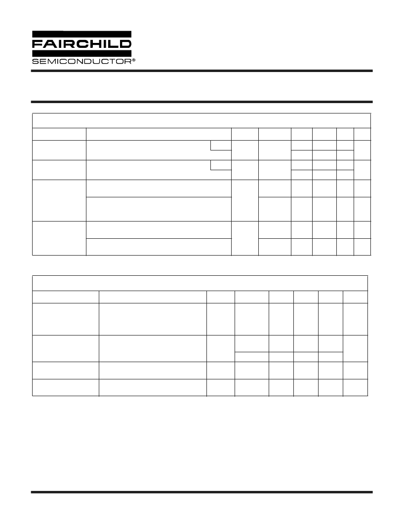
SWITCHING CHARACTERISTICS
(T
A
= 0 to 70°C unless otherwise specified., V
CC
= 3.3 V)
Parameter
Test Conditions
Symbol
Device
Min
Typ**
Max
Unit
Propagation delay
time to logic low
(R
L
= 1.9 k
, I
F
= 16 mA) (Note 2) (Fig. 10)
25°C
T
PHL
All
—
—
1.0
μs
—
—
2.0
Propagation delay
time to logic high
(R
L
= 1.9 k
, I
F
= 16 mA) (Note 2) (Fig. 10)
25°C
T
PLH
All
—
—
1.0
μs
—
—
2.0
Common mode
transient
immunity at
logic high
(I
F
= 0 mA, V
CM
(Note 3, 4) (Fig. 11) T
= 1,000 V
P-P
, R
L
= 4.1 k
= 25°C
)
A
|CM
H
|
All
5,000
50,000
—
V/μs
(I
F
= 0 mA, V
T
A
= 25°C, (R
L
= 1.9 k
)
(Note 2, 4) (Fig. 11)
CM
= 1,000 V
P-P
)
All
5,000
50,000
—
V/μs
Common mode
transient
immunity at
logic low
(I
F
= 16 mA, V
CM
= 1,000 V
P-P
, R
L
= 4.1 k
)
(Note 3, 4) (Fig. 11) T
A
= 25°C
(I
F
= 16 mA, V
CM
= 1,000 V
P-P
) (R
L
= 1.9 k
)
|CM
L
|
All
5,000
35,000
—
V/μs
(Note 2, 4) (Fig. 11)
All
5,000
35,000
—
V/μs
ISOLATION CHARACTERISTICS
(T
A
= 0 to 70°C Unless otherwise specified)
Characteristics
Test Conditions
Symbol
Device
Min
Typ**
Max
Unit
Input-output
insulation leakage
current
(Relative humidity = 45%)
(T
A
= 25°C, t = 5 s)
(V
I-O
= 3000 VDC)
(Note 5)
I
I-O
All
—
—
1.0
μA
Withstand insulation
test voltage
(f = 60 Hz, T
A
= 25°C)
(Note 5) ( t = 1 min.)
V
ISO
FOD050L
FOD053L
2500
—
—
V
RMS
FOD250L
5000
—
—
Resistance
(input to output)
(Note 5) (V
I-O
= 500 VDC)
R
I-O
All
10
11
10
12
—
Capacitance
(input to output)
(Note 5) (f = 1 MHz)
C
I-O
All
—
0.2
—
pF
相關(guān)PDF資料 |
PDF描述 |
|---|---|
| FOD053L | HIGH SPEED TRANSISTOR OPTOCOUPLERS |
| FOD060L | SSR OCMOS FET 200MA NO 6-DIP |
| FOD260L | LVTTL/LVCMOS 3.3V High Speed-10 MBit/s Logic Gate Optocouplers |
| FOD063L | LVTTL/LVCMOS 3.3V High Speed-10 MBit/s Logic Gate Optocouplers |
| FOD2200 | LOW INPUT CURRENT LOGIC GATE OPTOCOUPLERS |
相關(guān)代理商/技術(shù)參數(shù) |
參數(shù)描述 |
|---|---|
| FOD250LR1 | 制造商:FAIRCHILD 制造商全稱:Fairchild Semiconductor 功能描述:LVTTL/LVCMOS 3.3V High Speed Transistor Optocouplers |
| FOD250LR1V | 制造商:FAIRCHILD 制造商全稱:Fairchild Semiconductor 功能描述:LVTTL/LVCMOS 3.3V High Speed Transistor Optocouplers |
| FOD250LR2 | 制造商:FAIRCHILD 制造商全稱:Fairchild Semiconductor 功能描述:LVTTL/LVCMOS 3.3V High Speed Transistor Optocouplers |
| FOD250LR2V | 制造商:FAIRCHILD 制造商全稱:Fairchild Semiconductor 功能描述:LVTTL/LVCMOS 3.3V High Speed Transistor Optocouplers |
| FOD250LS | 功能描述:高速光耦合器 1Mbit/s HS Single Trans Output 3.3V RoHS:否 制造商:Avago Technologies 電流傳遞比: 最大波特率: 最大正向二極管電壓:1.75 V 最大反向二極管電壓:5 V 最大功率耗散:40 mW 最大工作溫度:+125 C 最小工作溫度:- 40 C 封裝 / 箱體:SOIC-5 封裝:Tube |
發(fā)布緊急采購,3分鐘左右您將得到回復(fù)。