- 您現(xiàn)在的位置:買賣IC網(wǎng) > PDF目錄370213 > FMS7950KWC Miscellaneous Clock Generator PDF資料下載
參數(shù)資料
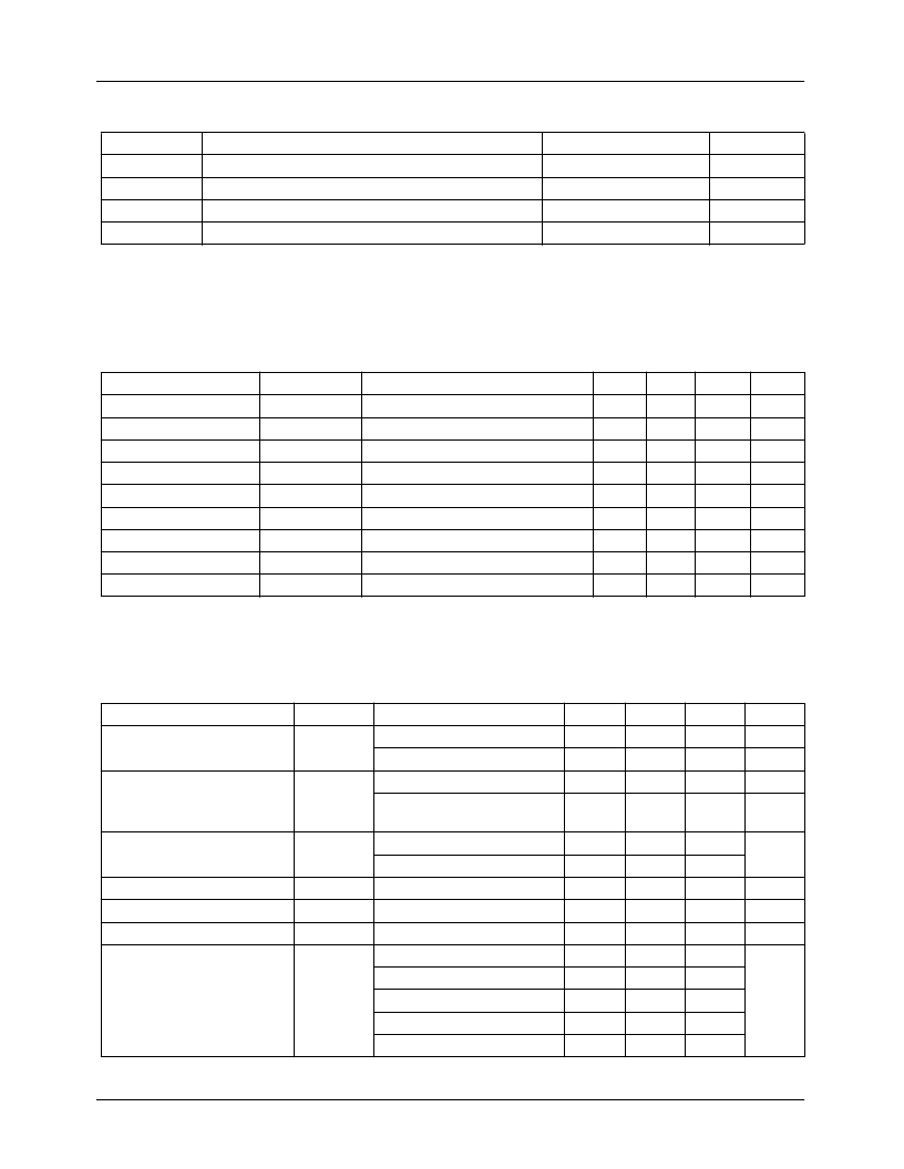
| 型號: | FMS7950KWC |
| 英文描述: | Miscellaneous Clock Generator |
| 中文描述: | 雜項時鐘發(fā)生器 |
| 文件頁數(shù): | 4/9頁 |
| 文件大小: | 72K |
| 代理商: | FMS7950KWC |
PRODUCT SPECIFICATION
FMS7950
4
REV. 1.0.0 1/9/01
Absolute Maximum Ratings
Stresses greater than those listed in the table may cause permanent damage to the device. These represent a stress rating only.
Operation of the device at these or any other conditions above those specified in the operating sections of this specification is
not implied. Maximum conditions for extended periods may effect reliability.
DC Electrical Characteristics
T
A
= 0 to 70°C; Supply Voltage 3.3 V ±0.2V (unless otherwise stated)
Parameter
Symbol
Input Low Voltage
V
IL
Input High Voltage
V
IH
Input Low Current
I
IL
Input High Current
I
IH
Output Low Voltage
V
OL
Output High Voltage
V
OH
Input Capacitance
C
IN
Supply Current
I
DD
Clock Stabilization
T
STAB
Note:
1. Guaranteed by design, not subject to 100% production testing.
AC Electrical Characteristics
T
A
= 0 to 70°C; Supply Voltage V
Parameter
Input Frequency Range
DD
Symbol
F
INPUT
= 3.3V ±0.2V, C
L
= 10 pF (unless otherwise stated)
Note:
1. Guaranteed by design, not subject to 100% production testing.
Symbol
V
DD
T
STG
T
B
T
A
Parameter
Ratings
-0.5 to 7.0
-65 to 150
-55 to 125
0 to 70
Units
V
°C
°C
°C
, V
IN
Voltage on any pin with respect to ground
Storage Temperature
Ambient Temperature
Operating Temperature
Conditions
Min.
Typ.
Max.
0.8
Units
V
V
μA
μA
V
V
pF
mA
mS
2.0
-10
-30
V
V
I
OL
I
OH
IN
= 0
= V
= 40 mA
= –40mA
10
30
0.5
IN
DD
2.2
(1)
7.0
200
10
Outputs loaded
From V
DD
(1)
= 3.3V to 1% Target
Conditions
FBsel = 1
FBsel = 0
Q
A
; DIV_SEL A = 0V
Q
B
, Q
C
& Q
DIV_SEL B, C, D = 0V
V
TH
= V
DD
/2; DIV_SEL A = 0
V
TH
= V
DD
/2; DIV_SEL A = 1
0.8 to 2.0V
2.0 to 0.8V
V
TH
= V
DD
/2
QA: DIV_SEL A = 0
QA: DIV_SEL A = 1
QB Output
QC(0:1) Outputs
QD(0:4) Outputs
Min.
25
12
Typ.
Max.
43
22
175
88
Units
MHz
MHz
MHz
MHz
Output Frequency Range
F
OUT
D
;
Output to Output Skew
T
SK1
400
100
750
300
1.0
1.0
55
450
200
200
300
375
pS
-300
0.10
0.10
45
Rise Time
Fall Time
Duty Cycle
Jitter (Cycle-Cycle)
(1)
T
T
D
T
R
nS
nS
%
pS
(1)
F
(1)
T
JIT
相關PDF資料 |
PDF描述 |
|---|---|
| FMS7950KWCX | Miscellaneous Clock Generator |
| FMS7951KWC | Nine Distributed-Output Clock Driver |
| FMS7951KWCX | Nine Distributed-Output Clock Driver |
| FMS9875KGC100 | |
| FMS9875KGC100X | 1-Bit Bidirectional Voltage-Level Translator With Auto Direction Sensing and +/-15-kV ESD Protect 6-SOT -40 to 85 |
相關代理商/技術參數(shù) |
參數(shù)描述 |
|---|---|
| FMS7950KWCX | 制造商:未知廠家 制造商全稱:未知廠家 功能描述:Miscellaneous Clock Generator |
| FMS7951 | 制造商:FAIRCHILD 制造商全稱:Fairchild Semiconductor 功能描述:Zero Delay Clock Multiplier |
| FMS7951KWC | 制造商:Rochester Electronics LLC 功能描述:- Bulk |
| FMS7951KWCX | 制造商:未知廠家 制造商全稱:未知廠家 功能描述:Nine Distributed-Output Clock Driver |
| FMS7G10US60 | 功能描述:視頻 IC Compact Module Complex RoHS:否 制造商:Fairchild Semiconductor 工作電源電壓:5 V 電源電流:80 mA 最大工作溫度:+ 85 C 封裝 / 箱體:TSSOP-28 封裝:Reel |
發(fā)布緊急采購,3分鐘左右您將得到回復。