- 您現(xiàn)在的位置:買(mǎi)賣(mài)IC網(wǎng) > PDF目錄375850 > FM34W02ULZEM8 (FAIRCHILD SEMICONDUCTOR CORP) I2C Serial EEPROM PDF資料下載
參數(shù)資料
| 型號(hào): | FM34W02ULZEM8 |
| 廠商: | FAIRCHILD SEMICONDUCTOR CORP |
| 元件分類(lèi): | DRAM |
| 英文描述: | I2C Serial EEPROM |
| 中文描述: | 256 X 8 I2C/2-WIRE SERIAL EEPROM, PDSO8 |
| 封裝: | PLASTIC, SO-8 |
| 文件頁(yè)數(shù): | 5/12頁(yè) |
| 文件大?。?/td> | 95K |
| 代理商: | FM34W02ULZEM8 |
5
www.fairchildsemi.com
FM34W02U Rev. A.1
F
w
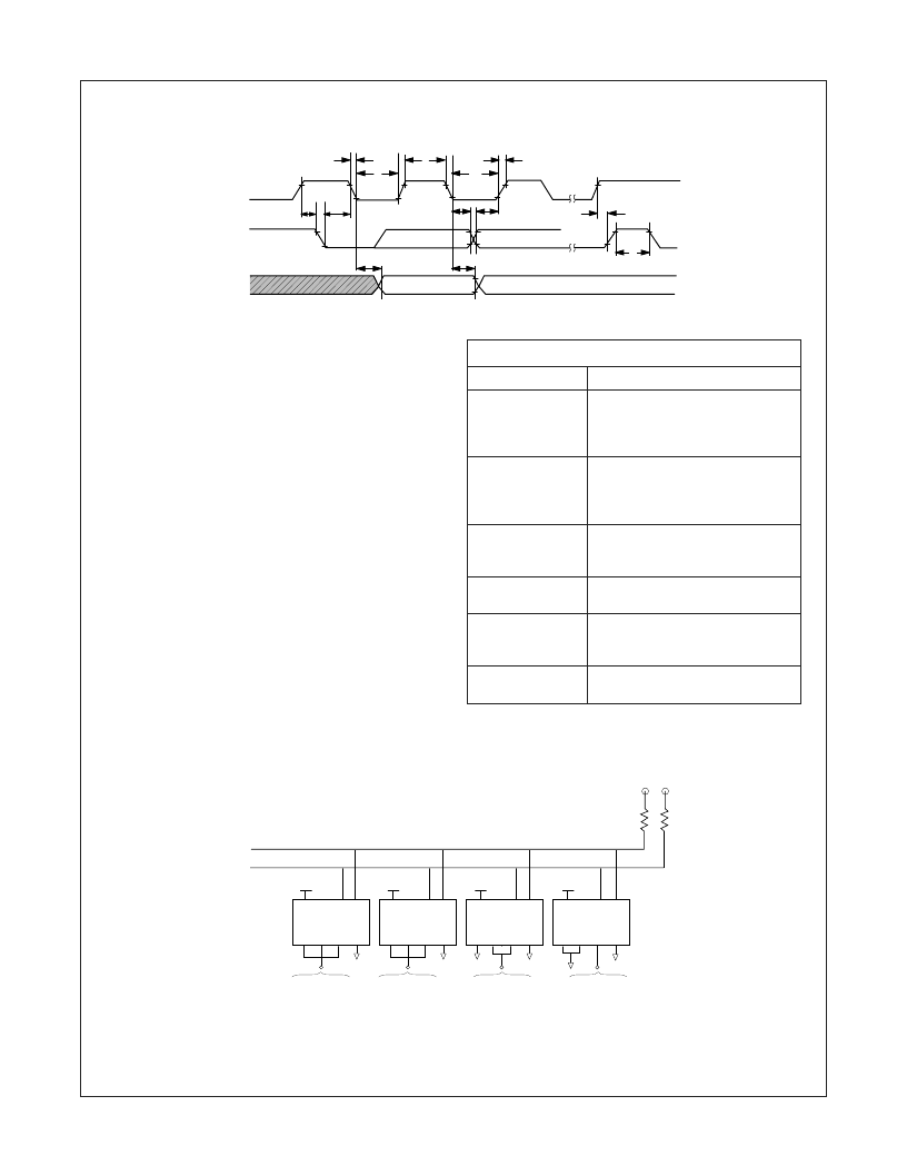
Bus Timing
Background Information (IIC Bus)
As mentioned, the IIC bus allows synchronous bidirectional com-
munication between Transmitter/Receiver using the SCL (clock)
and SDA (Data I/O) lines. All communication must be started with
a valid START condition, concluded with a STOP condition and
acknowledged by the Receiver with an ACKNOWLEDGE condi-
tion.
In addition, since the IIC bus is designed to support other devices
such as RAM, EPROMs, etc., a device type identifier string must
follow the START condition. For EEPROMs, this 4-bit string is
1010. Also refer the
Addressing the WP Register
section.
As shown below, although the EEPROMs on the IIC bus may be
configured in any manner required, the total memory addressed
can not exceed 16K (16,384 bits) on the Standard IIC. EEPROM
memory address programming is controlled by 2 methods:
Hardware configuring the A0, A1, and A2 pins (Device
Address pins) with pull-up or pull-down to V
CC
or V
SS
.
All
unused pins must be grounded
(tied to V
SS
).
Software addressing the required PAGE BLOCK within the
device memory array (as sent in the Slave Address string).
Addressing an EEPROM memory location involves sending a
command string with the following information:
[DEVICE TYPE]
—
[DEVICE ADDRESS]
—
[PAGE BLOCK
ADDRESS]
—
[BYTE ADDRESS]
DEFINITIONS
BYTE
8 bits of data
PAGE
16 sequential addresses (one byte
each) that may be programmed
during a 'Page Write' programming
cycle
PAGE BLOCK
2,048 (2K) bits organized into 16
pages of addressable memory. (8
bits) x (16 bytes) x (16 pages) = 2,048
bits
MASTER
Any IIC device CONTROLLING the
transfer of data (such as a micropro-
cessor)
SLAVE
Device being controlled (EEPROMs
are always considered Slaves)
TRANSMITTER
Device currently SENDING data on
the bus (may be either a Master or
Slave).
RECEIVER
Device currently receiving data on the
bus (Master or Slave)
Example of 16K of Memory on 2-Wire Bus
Note:
The SDA pull-up resistor is required due to the open-drain/open collector output of IIC bus devices.
The SCL pull-up resistor is recommended because of the normal SCL line inactive 'high' state.
It is recommended that the total line capacitance be less than 400pF.
Specific timing and addressing considerations are described in greater detail in the following sections.
SCL
SDA
IN
SDA
OUT
tF
tLOW
tHIGH
tR
tLOW
tAA
tDH
tBUF
tSU:STA
tHD:DAT
tHD:STA
tSU:DAT
tSU:STO
SDA
SCL
34C02L
VCC
VCC
A0 A1 A2 VSS
24C02
A0 A1 A2 VSS
24C04
A0 A1 A2 VSS
24C08
A0 A1 A2 VSS
VCC
To VCC or VSS
To VCC or VSS
To VCC or VSS
To VCC or VSS
VCC
VCC
VCC
相關(guān)PDF資料 |
PDF描述 |
|---|---|
| FM34W02ULZEMT8 | I2C Serial EEPROM |
| FM34W02ULZM8 | I2C Serial EEPROM |
| FM34W02ULZMT8 | I2C Serial EEPROM |
| FM34W02UM8 | I2C Serial EEPROM |
| FM34W02UMT8 | I2C Serial EEPROM |
相關(guān)代理商/技術(shù)參數(shù) |
參數(shù)描述 |
|---|---|
| FM34W02ULZEMT8 | 功能描述:電可擦除可編程只讀存儲(chǔ)器 RoHS:否 制造商:Atmel 存儲(chǔ)容量:2 Kbit 組織:256 B x 8 數(shù)據(jù)保留:100 yr 最大時(shí)鐘頻率:1000 KHz 最大工作電流:6 uA 工作電源電壓:1.7 V to 5.5 V 最大工作溫度:+ 85 C 安裝風(fēng)格:SMD/SMT 封裝 / 箱體:SOIC-8 |
| FM34W02ULZEMT8X | 功能描述:電可擦除可編程只讀存儲(chǔ)器 RoHS:否 制造商:Atmel 存儲(chǔ)容量:2 Kbit 組織:256 B x 8 數(shù)據(jù)保留:100 yr 最大時(shí)鐘頻率:1000 KHz 最大工作電流:6 uA 工作電源電壓:1.7 V to 5.5 V 最大工作溫度:+ 85 C 安裝風(fēng)格:SMD/SMT 封裝 / 箱體:SOIC-8 |
| FM34W02ULZM8 | 制造商:FAIRCHILD 制造商全稱(chēng):Fairchild Semiconductor 功能描述:I2C Serial EEPROM |
| FM34W02ULZMT8 | 制造商:FAIRCHILD 制造商全稱(chēng):Fairchild Semiconductor 功能描述:I2C Serial EEPROM |
| FM34W02UM8 | 功能描述:電可擦除可編程只讀存儲(chǔ)器 SOIC-8 RoHS:否 制造商:Atmel 存儲(chǔ)容量:2 Kbit 組織:256 B x 8 數(shù)據(jù)保留:100 yr 最大時(shí)鐘頻率:1000 KHz 最大工作電流:6 uA 工作電源電壓:1.7 V to 5.5 V 最大工作溫度:+ 85 C 安裝風(fēng)格:SMD/SMT 封裝 / 箱體:SOIC-8 |
發(fā)布緊急采購(gòu),3分鐘左右您將得到回復(fù)。