- 您現(xiàn)在的位置:買(mǎi)賣(mài)IC網(wǎng) > PDF目錄375799 > FIN24AGFX (FAIRCHILD SEMICONDUCTOR CORP) Low Voltage 24-Bit Bi-Directional Serializer/Deserializer with Multiple Frequency Ranges (Preliminary) PDF資料下載
參數(shù)資料
| 型號(hào): | FIN24AGFX |
| 廠商: | FAIRCHILD SEMICONDUCTOR CORP |
| 元件分類(lèi): | 通用總線功能 |
| 英文描述: | Low Voltage 24-Bit Bi-Directional Serializer/Deserializer with Multiple Frequency Ranges (Preliminary) |
| 中文描述: | LINE TRANSCEIVER, PBGA42 |
| 封裝: | 3.50 MM, LEAD FREE, MO-195, BGA-42 |
| 文件頁(yè)數(shù): | 7/20頁(yè) |
| 文件大小: | 1758K |
| 代理商: | FIN24AGFX |
第1頁(yè)第2頁(yè)第3頁(yè)第4頁(yè)第5頁(yè)第6頁(yè)當(dāng)前第7頁(yè)第8頁(yè)第9頁(yè)第10頁(yè)第11頁(yè)第12頁(yè)第13頁(yè)第14頁(yè)第15頁(yè)第16頁(yè)第17頁(yè)第18頁(yè)第19頁(yè)第20頁(yè)

Preliminary
7
www.fairchildsemi.com
F
Embedded Word Clock Operation
The FIN24A sends and receives serial data source syn-
chronously with a bit clock. The bit clock has been modified
to create a word boundary at the end of each data word.
The word boundary has been implemented by skipping a
low clock pulse. This appears in the serial clock stream as
3 consecutive bit times where signal CKSO remains HIGH.
In order to implement this sort of scheme two extra data
bits are required. During the word boundary phase the data
will toggle either HIGH-then-LOW or LOW-then-HIGH
dependent upon the last bit of the actual data word. Table 2
provides some examples showing the actual data word and
the data word with the word boundary bits added. Note that
a 24-bit word will be extended to 26-bits during serial trans-
mission. Bit 25 and Bit 26 are defined with-respect-to Bit
24. Bit 25 will always be the inverse of Bit 24, and Bit 26
will always be the same as Bit 24. This insures that a
“
0
”
o
“
1
”
and a
“
1
”
o
“
0
”
transition will always occur during
the embedded word phase where CKSO is HIGH.
The serializer generates the word boundary data bits and
the boundary clock condition and embeds them into the
serial data stream. The deserializer looks for the end of the
word boundary condition to capture and transfer the data to
the parallel port. The deserializer only uses the embedded
word boundary information to find and capture the data.
These boundary bits are then stripped prior to the word
being sent out of the parallel port.
TABLE 2. Word Boundary Data Bits
LVCMOS Data I/O
The LVCMOS input buffers have a nominal threshold value
equal to
of V
DDP
. The input buffers are only operational
when the device is operating as a serializer. When the
device is operating as a deserializer the inputs are gated
off to conserve power.
The LVCMOS 3-STATE output buffers are rated for a
source/sink current of 2 mAs at 1.8V. The outputs are
active when the DIRI signal is asserted LOW. When the
DIRI signal is asserted HIGH the bi-directional LVCMOS
I/Os will be in a HIGH-Z state. Under purely capacitive load
conditions the output will swing between GND and V
DDP
.
The LVCMOS I/O buffers incorporate bushold functionality
to allow for pins to maintain state when they are not driven.
The bushold circuitry only consumes power during signal
transitions.
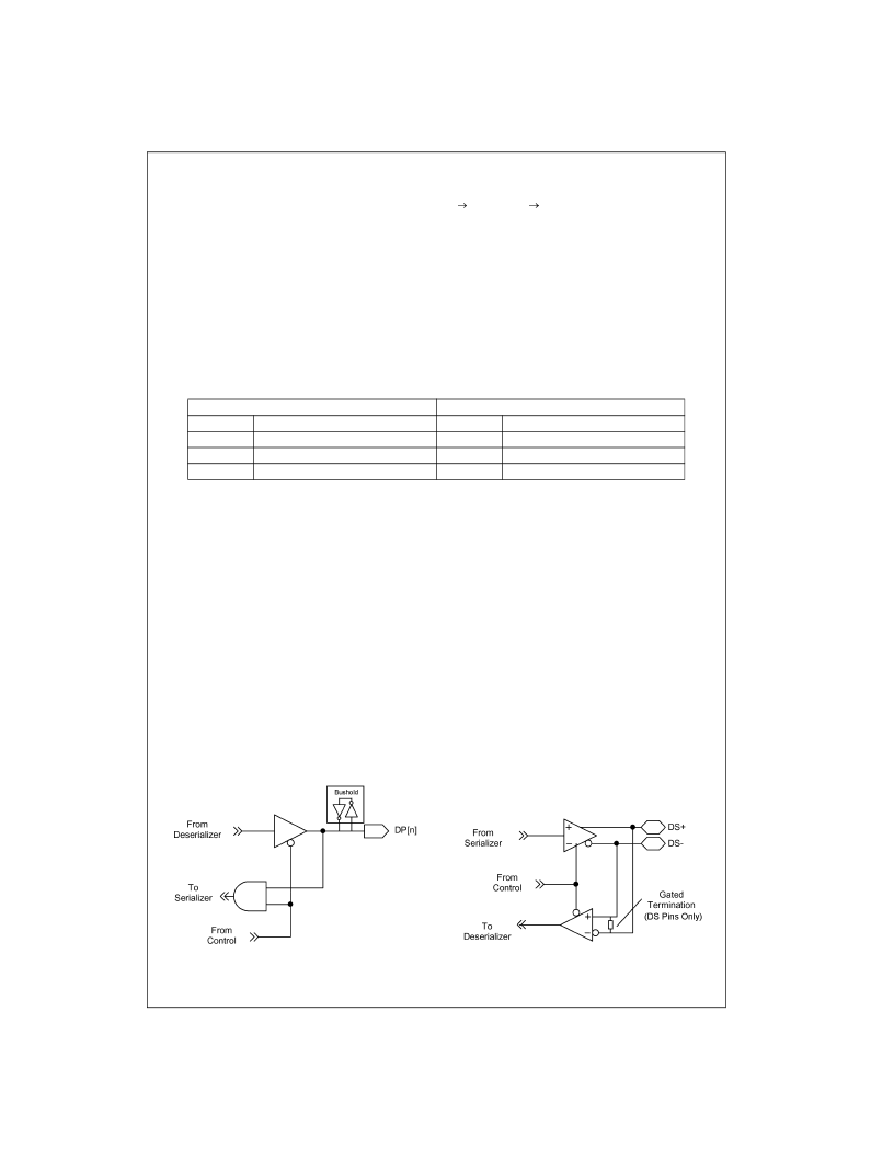
FIGURE 6. LVCMOS I/O
Differential I/O Circuitry
The differential I/O circuitry is a low power variant of LVDS.
The differential outputs operate in the same fashion as
LVDS by sourcing and sinking a balanced current through
the output pair. Like LVDS an input source termination
resistor is required to develop a voltage at the differential
input pair. The FIN24A device incorporates an internal ter-
mination resistor on the CKSI receiver and a gated internal
termination resistor on the DS input receiver. The gated ter-
mination resistor insures proper termination regardless of
direction of data flow.
During power-down mode the differential inputs will be dis-
abled and powered down and the differential outputs will be
placed in a HIGH-Z state.
FIGURE 7. Bi-directional Differential I/O Circuitry
24-Bit Data Words
24-Bit Data Word with Word Boundary
Hex
1FFFFFFh
01 1111 1111 1111 1111 1111 1111b
1155555h
01 0101 0101 0101 0101 0101 0101b
1xxxxxxh
01 0xxx xxxx xxxx xxxx xxxx xxxxb
Hex
Binary
Binary
3FFFFFh
155555h
xxxxxxh
0011 1111 1111 1111 1111 1111b
0101 0101 0101 0101 01010 0101b
0xxx xxxx xxxx xxxx xxxx xxxxb
相關(guān)PDF資料 |
PDF描述 |
|---|---|
| FIN24AMLX | Low Voltage 24-Bit Bi-Directional Serializer/Deserializer with Multiple Frequency Ranges (Preliminary) |
| FIN24C | uSerDes Low Voltage 24-Bit Bi-Directional Serializer/Deserializer |
| FIN24CGFX | uSerDes Low Voltage 24-Bit Bi-Directional Serializer/Deserializer |
| FIN24CMLX | uSerDes Low Voltage 24-Bit Bi-Directional Serializer/Deserializer |
| FIN3383 | 2MM TERMINAL STRIPS |
相關(guān)代理商/技術(shù)參數(shù) |
參數(shù)描述 |
|---|---|
| FIN24AMLX | 制造商:FAIRCHILD 制造商全稱(chēng):Fairchild Semiconductor 功能描述:Low Voltage 24-Bit Bi-Directional Serializer/Deserializer with Multiple Frequency Ranges (Preliminary) |
| FIN24C | 制造商:FAIRCHILD 制造商全稱(chēng):Fairchild Semiconductor 功能描述:uSerDes⑩Low-Voltage 24-Bit Bi-Directional Serializer/Deserializer |
| FIN24C_06 | 制造商:FAIRCHILD 制造商全稱(chēng):Fairchild Semiconductor 功能描述:uSerDes⑩Low-Voltage 24-Bit Bi-Directional Serializer/Deserializer |
| FIN24CGFX | 功能描述:LVDS 接口集成電路 SerDes LV 24-Bit Bi RoHS:否 制造商:Texas Instruments 激勵(lì)器數(shù)量:4 接收機(jī)數(shù)量:4 數(shù)據(jù)速率:155.5 Mbps 工作電源電壓:5 V 最大功率耗散:1025 mW 最大工作溫度:+ 85 C 封裝 / 箱體:SOIC-16 Narrow 封裝:Reel |
| FIN24CMLX | 功能描述:LVDS 接口集成電路 SerDes LV 24-Bit Bi RoHS:否 制造商:Texas Instruments 激勵(lì)器數(shù)量:4 接收機(jī)數(shù)量:4 數(shù)據(jù)速率:155.5 Mbps 工作電源電壓:5 V 最大功率耗散:1025 mW 最大工作溫度:+ 85 C 封裝 / 箱體:SOIC-16 Narrow 封裝:Reel |
發(fā)布緊急采購(gòu),3分鐘左右您將得到回復(fù)。