- 您現(xiàn)在的位置:買賣IC網(wǎng) > PDF目錄375765 > FDP6670S (FAIRCHILD SEMICONDUCTOR CORP) 30V N-Channel PowerTrench? SyncFET PDF資料下載
參數(shù)資料
| 型號(hào): | FDP6670S |
| 廠商: | FAIRCHILD SEMICONDUCTOR CORP |
| 元件分類: | JFETs |
| 英文描述: | 30V N-Channel PowerTrench? SyncFET |
| 中文描述: | 62 A, 30 V, 0.0085 ohm, N-CHANNEL, Si, POWER, MOSFET, TO-220AB |
| 封裝: | TO-220, 3 PIN |
| 文件頁數(shù): | 2/6頁 |
| 文件大小: | 93K |
| 代理商: | FDP6670S |
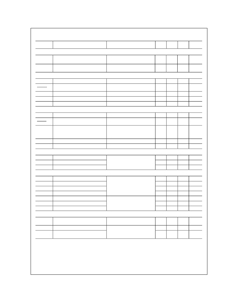
FDP6670S/FDB6670S Rev E (W)
Electrical Characteristics
Symbol
T
A
= 25°C unless otherwise noted
Test Conditions
Parameter
Min Typ Max Units
Drain-Source Avalanche Ratings
(Note 1)
W
DSS
Single Pulse Drain-Source
Avalanche Energy
V
DD
= 25 V,
I
D
= 16.5 A
285
16.5
mJ
I
AR
Maximum Drain-Source Avalanche
Current
A
Off Characteristics
BV
DSS
Drain–Source Breakdown Voltage
BV
DSS
T
J
Coefficient
I
DSS
Zero Gate Voltage Drain Current
I
GSSF
Gate–Body Leakage, Forward
I
GSSR
Gate–Body Leakage, Reverse
On Characteristics
V
GS(th)
Gate Threshold Voltage
V
GS(th)
T
J
Temperature Coefficient
R
DS(on)
Static Drain–Source
On–Resistance
V
GS
= 0 V,
I
D
= 1mA
30
V
Breakdown Voltage Temperature
I
D
= 26mA, Referenced to 25
°
C
24
mV/
°
C
V
DS
= 24 V,
V
GS
= 20 V,
V
GS
= –20 V, V
DS
= 0 V
V
GS
= 0 V
V
DS
= 0 V
500
μA
100
–100
nA
nA
(Note 2)
V
DS
= V
GS
,
I
D
= 26mA, Referenced to 25
°
C
V
GS
= 10 V, I
D
= 31 A
V
GS
= 4.5 V, I
D
= 26.5 A
V
GS
=10 V, I
D
=31 A, T
J
=125
°
C
V
GS
= 10 V,
V
DS
= 10 V
V
DS
= 10 V, I
D
= 31 A
I
D
= 1mA
1
2.2
–4.5
5
8
10
3
V
Gate Threshold Voltage
mV/
°
C
8.5
12.5
19
m
I
D(on)
g
FS
On–State Drain Current
Forward Transconductance
60
A
S
69
Dynamic Characteristics
C
iss
Input Capacitance
C
oss
Output Capacitance
C
rss
Reverse Transfer Capacitance
Switching Characteristics
t
d(on)
Turn–On Delay Time
t
r
Turn–On Rise Time
t
d(off)
Turn–Off Delay Time
t
f
Turn–Off Fall Time
Q
g
Total Gate Charge
Q
gs
Gate–Source Charge
Q
gd
Gate–Drain Charge
Drain–Source Diode Characteristics
V
SD
Drain–Source Diode Forward
Voltage
t
rr
Diode Reverse Recovery Time
Q
rr
Diode Reverse Recovery Charge
2639
737
222
pF
pF
pF
V
DS
= 15 V, V
GS
= 0 V,
f = 1.0 MHz
(Note 2)
13
24
ns
10
39
35
23
21
62
56
32
ns
ns
ns
nC
V
DS
= 15 V,
V
GS
= 10 V,
I
D
= 1 A,
R
GEN
= 6
9
8
nC
nC
V
DS
= 15 V, I
D
= 31 A,
V
GS
= 5 V
V
GS
= 0 V,
V
GS
= 0 V,
I
F
= 3.5 A,
d
iF
/d
t
= 300 A/μs
I
S
= 3.5 A
I
S
= 7 A
(Note 1)
(Note 1)
0.39
0.48
32
0.7
0.9
V
nS
(Note 2)
56
nC
Notes:
1.
Pulse Test: Pulse Width < 300
μ
s, Duty Cycle < 2.0%
2.
See “SyncFET Schottky body diode characteristics” below.
F
相關(guān)PDF資料 |
PDF描述 |
|---|---|
| FDB6676S | 30V N-Channel PowerTrench SyncFET⑩ |
| FDP6676S | 30V N-Channel PowerTrench SyncFET⑩ |
| FDB6676 | 30V N-Channel Logic Level PowerTrench MOSFET |
| FDP6676 | 30V N-Channel Logic Level PowerTrench MOSFET |
| FDB6690S | 30V N-Channel PowerTrench SyncFET |
相關(guān)代理商/技術(shù)參數(shù) |
參數(shù)描述 |
|---|---|
| FDP6676 | 功能描述:MOSFET 30V N-Ch PowerTrench Logic Level RoHS:否 制造商:STMicroelectronics 晶體管極性:N-Channel 汲極/源極擊穿電壓:650 V 閘/源擊穿電壓:25 V 漏極連續(xù)電流:130 A 電阻汲極/源極 RDS(導(dǎo)通):0.014 Ohms 配置:Single 最大工作溫度: 安裝風(fēng)格:Through Hole 封裝 / 箱體:Max247 封裝:Tube |
| FDP6676S | 功能描述:MOSFET 30V N-Ch PowerTrench RoHS:否 制造商:STMicroelectronics 晶體管極性:N-Channel 汲極/源極擊穿電壓:650 V 閘/源擊穿電壓:25 V 漏極連續(xù)電流:130 A 電阻汲極/源極 RDS(導(dǎo)通):0.014 Ohms 配置:Single 最大工作溫度: 安裝風(fēng)格:Through Hole 封裝 / 箱體:Max247 封裝:Tube |
| FDP6690 | 制造商:FAIRCHILD 制造商全稱:Fairchild Semiconductor 功能描述:30V N-Channel PowerTrench SyncFET |
| FDP6690S | 功能描述:MOSFET 30V N-Ch PowerTrench RoHS:否 制造商:STMicroelectronics 晶體管極性:N-Channel 汲極/源極擊穿電壓:650 V 閘/源擊穿電壓:25 V 漏極連續(xù)電流:130 A 電阻汲極/源極 RDS(導(dǎo)通):0.014 Ohms 配置:Single 最大工作溫度: 安裝風(fēng)格:Through Hole 封裝 / 箱體:Max247 封裝:Tube |
| FDP6N60ZU | 制造商:FAIRCHILD 制造商全稱:Fairchild Semiconductor 功能描述:N-Channel MOSFET, FRFET 600V, 4.5A, 2Ω |
發(fā)布緊急采購,3分鐘左右您將得到回復(fù)。