- 您現(xiàn)在的位置:買賣IC網(wǎng) > PDF目錄370147 > FAN8800 PDF資料下載
參數(shù)資料
| 型號: | FAN8800 |
| 文件頁數(shù): | 110/191頁 |
| 文件大?。?/td> | 2018K |
| 代理商: | FAN8800 |
第1頁第2頁第3頁第4頁第5頁第6頁第7頁第8頁第9頁第10頁第11頁第12頁第13頁第14頁第15頁第16頁第17頁第18頁第19頁第20頁第21頁第22頁第23頁第24頁第25頁第26頁第27頁第28頁第29頁第30頁第31頁第32頁第33頁第34頁第35頁第36頁第37頁第38頁第39頁第40頁第41頁第42頁第43頁第44頁第45頁第46頁第47頁第48頁第49頁第50頁第51頁第52頁第53頁第54頁第55頁第56頁第57頁第58頁第59頁第60頁第61頁第62頁第63頁第64頁第65頁第66頁第67頁第68頁第69頁第70頁第71頁第72頁第73頁第74頁第75頁第76頁第77頁第78頁第79頁第80頁第81頁第82頁第83頁第84頁第85頁第86頁第87頁第88頁第89頁第90頁第91頁第92頁第93頁第94頁第95頁第96頁第97頁第98頁第99頁第100頁第101頁第102頁第103頁第104頁第105頁第106頁第107頁第108頁第109頁當(dāng)前第110頁第111頁第112頁第113頁第114頁第115頁第116頁第117頁第118頁第119頁第120頁第121頁第122頁第123頁第124頁第125頁第126頁第127頁第128頁第129頁第130頁第131頁第132頁第133頁第134頁第135頁第136頁第137頁第138頁第139頁第140頁第141頁第142頁第143頁第144頁第145頁第146頁第147頁第148頁第149頁第150頁第151頁第152頁第153頁第154頁第155頁第156頁第157頁第158頁第159頁第160頁第161頁第162頁第163頁第164頁第165頁第166頁第167頁第168頁第169頁第170頁第171頁第172頁第173頁第174頁第175頁第176頁第177頁第178頁第179頁第180頁第181頁第182頁第183頁第184頁第185頁第186頁第187頁第188頁第189頁第190頁第191頁
FAN8026D (KA3026D)
8
D
Application Information
1. REFERENCE INPUT
Pin 12 (REF) is a reference Input pin.
1) Reference Input
The applied voltage at the reference input pin must be between 1.5 (V) and 6.5 (V), when Vcc = 8V.
2. SEPARATED CHANNEL MUTE FUNCTION
These pins are used for individual channel mute operation.
1) When the mute pins (pin13,14 and 22) are Low level, the mute circuits are enabled and the output circuits are muted.
2) When the voltage of the mute pins (pin13,14 and 22) are High level, the mute circuits are disabled and the output circuits
operate normally.
3) If the chip temperature rises above 175
°
C, then the thermal shutdown (TSD) circuit is activated and the output circuits are
muted.
Mute1, 2 (pin13) - CH1, 2 mute control input pin.
Mute3 (pin14) - CH3 mute control input pin.
Mute4 (pin22) - CH4 mute control input pin.
3. PROTECTION FUNCTION
Thermal Shutdown (TSD)
1) If the chip temperature rises above 175
°
C the thermal shutdown (TSD) circuit is activated and the output circuit is in the
Mute state, that is Off state.
The TSD circuit has a temperature hysteresis of 25
°
C.
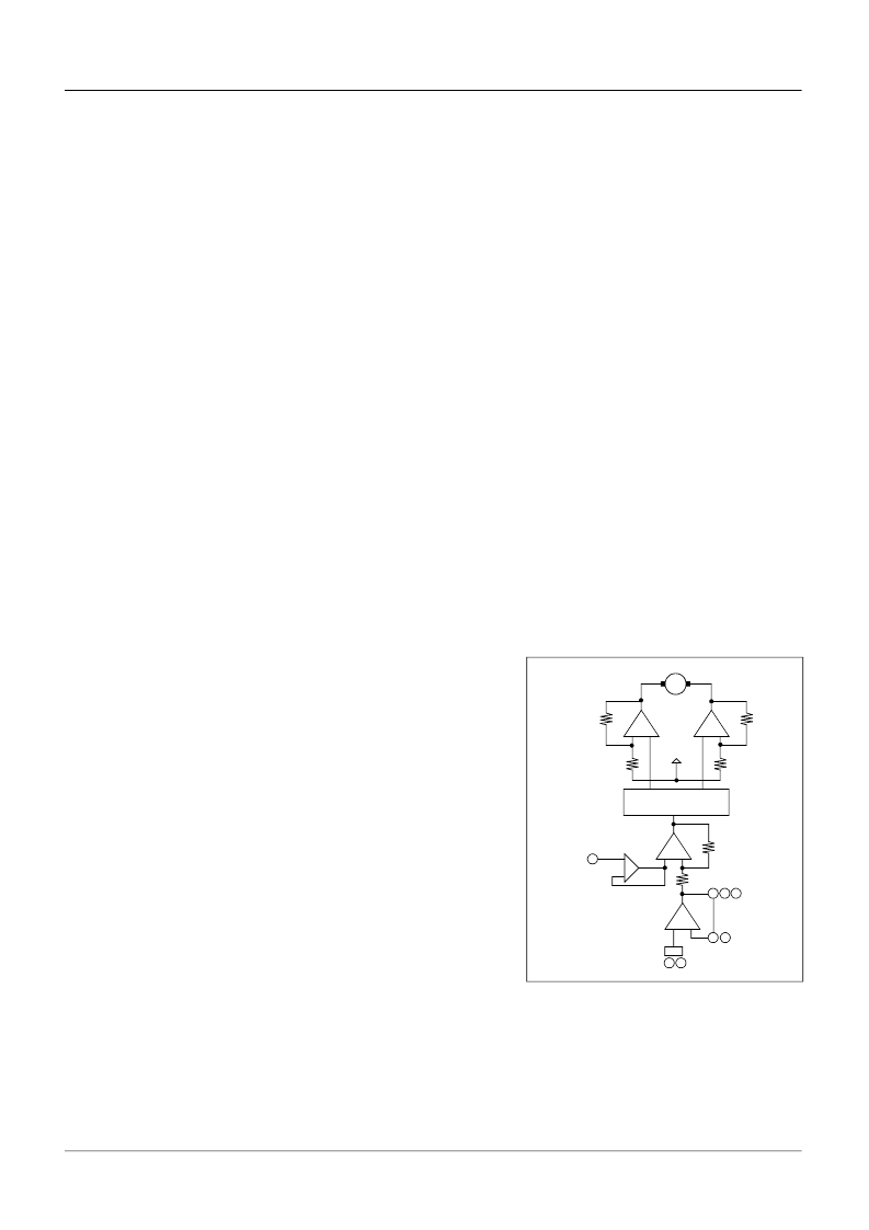
4. FOCUS, TRACKING ACTUATOR, SLED MOTOR DRIVE PART
1) The reference voltage REF is given externally through pin 12.
2) The error amp output signal is amplified by R2/R1 times and then fed to
the level shift circuit.
3) The level shift circuit produces the differential output voltages and drives
the two output power amplifiers.
Since the differential gain of the output amplifiers is equal to 2
×
(1+ R4/
R3), the output signal of the error amp is amplified by (R2/R1)
×
2
×
(1+R4/R3).
4) If the total gain is insufficient, the input error amp can be used to increase
the gain.
5) The bias voltage (Vr) is about a half of the supply voltage(VM).
-
+
LEVEL
SNIFT
Vin
1 4
2 5
3 6 7
EA
+
-
+
-
R1
R2
AP1
+
-
12
Vref
Error Amp
+
+
-
-
AP2
AP3
R3
R3
Vr
R4
R4
Power Amp
M
相關(guān)PDF資料 |
PDF描述 |
|---|---|
| FAN6555M | SMPS Controller |
| FAN6555MX | SMPS Controller |
| FAN7000DTF | Dual Audio Amplifier |
| FAN73832 | Half-Bridge Gate-Drive IC |
| FAN73832M | Half-Bridge Gate-Drive IC |
相關(guān)代理商/技術(shù)參數(shù) |
參數(shù)描述 |
|---|---|
| FAN8902 | 功能描述:馬達(dá)/運(yùn)動(dòng)/點(diǎn)火控制器和驅(qū)動(dòng)器 Fan Motor Controller DC RoHS:否 制造商:STMicroelectronics 產(chǎn)品:Stepper Motor Controllers / Drivers 類型:2 Phase Stepper Motor Driver 工作電源電壓:8 V to 45 V 電源電流:0.5 mA 工作溫度:- 25 C to + 125 C 安裝風(fēng)格:SMD/SMT 封裝 / 箱體:HTSSOP-28 封裝:Tube |
| FAN8903 | 制造商:FAIRCHILD 制造商全稱:Fairchild Semiconductor 功能描述:Power Window Motor Control IC |
| FAN9100_ZBA3026B WAF | 制造商:Fairchild Semiconductor Corporation 功能描述: |
| FAN9116Z WAF | 制造商:Fairchild Semiconductor Corporation 功能描述: |
| FAN9611 | 制造商:Fairchild 功能描述:INTERLEAVED PFC IC |
發(fā)布緊急采購,3分鐘左右您將得到回復(fù)。