- 您現(xiàn)在的位置:買賣IC網(wǎng) > PDF目錄375726 > FAN6520AMX (FAIRCHILD SEMICONDUCTOR CORP) Single Synchronous Buck PWM Controller PDF資料下載
參數(shù)資料
| 型號: | FAN6520AMX |
| 廠商: | FAIRCHILD SEMICONDUCTOR CORP |
| 元件分類: | 穩(wěn)壓器 |
| 英文描述: | Single Synchronous Buck PWM Controller |
| 中文描述: | 1 A SWITCHING CONTROLLER, 340 kHz SWITCHING FREQ-MAX, PDSO8 |
| 封裝: | MS-012AA, SOIC-8 |
| 文件頁數(shù): | 10/15頁 |
| 文件大小: | 580K |
| 代理商: | FAN6520AMX |

10
REV. 1.0.2 8/26/04
FAN6520A
PRODUCT SPECIFICATION
RMS current required by the circuit. The capacitor voltage
rating should be at least 1.25 times greater than the maxi-
mum input voltage and a voltage rating of 1.5 times is a
conservative guideline.
The RMS current rating requirement (I
RMS
) for the input
capacitor of a buck regulator is:
where the converter duty cycle;
. For a
through-hole design, several electrolytic capacitors may be
needed. For surface-mount designs, solid tantalum capaci-
tors can be used, but caution must be exercised with regard
to the capacitor’s surge current rating. The capacitors must
be capable of handling the surge current at power-up. Some
capacitor series available from reputable manufacturers are
surge current tested.
Bootstrap Circuit
The bootstrap circuit uses a charge storage capacitor
(C
BOOT
) and the internal diode, as shown in Figure 1.
Selection of these components should be done after the
high-side MOSFET has been chosen. The required
capacitance is determined using the following equation:
where Q
G
is the total gate charge of the high-side MOSFET,
and
V
BOOT
is the voltage droop allowed on the high-side
MOSFET drive. To prevent loss of gate drive, the bootstrap
capacitance should be at least 50 times greater than the C
ISS
of Q1.
Thermal Considerations
Total device dissipation:
P
D
= P
Q
+ P
HDRV
+ P
LDRV
(4)
where P
Q
represents quiescent power dissipation:
P
Q
= V
CC
×
[4mA + 0.036 (F
SW
– 100)]
(5)
where F
SW
is switching frequency (in kHz).
P
HDRV
represents internal power dissipation of the upper
FET driver.
P
HDRV
= P
H(R)
×
P
H(F)
(6)
Where P
H(R)
and P
H(F)
are internal dissipations for the
rising and falling edges respectively:
where:
P
Q1
= Q
G1
×
V
GS(Q1)
×
F
SW
(9)
Where Q
G1
is total gate charge of Q1 for its applied V
GS
.
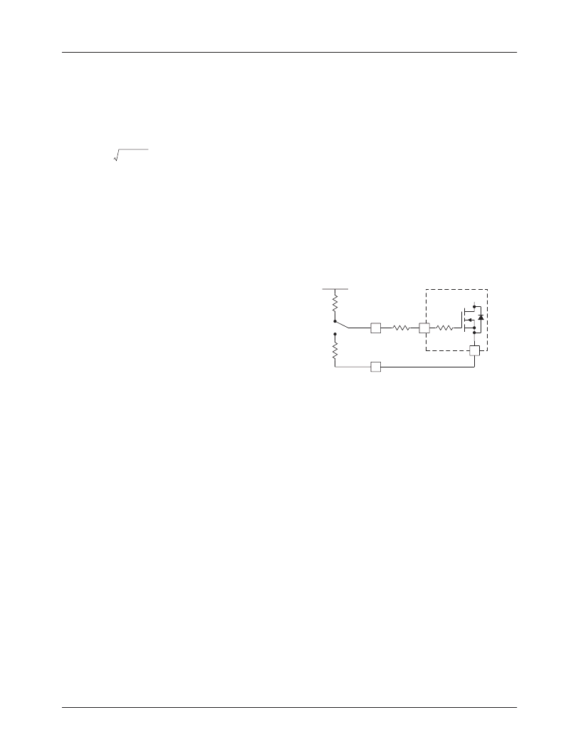
As described in the equations above, the total power con-
sumed in driving the gate is divided in proportion to the
resistances in series with the MOSFET's internal gate node
as shown in Figure 9.
Figure 9. Driver Dissipation Model
R
G
is the polysilicon gate resistance, internal to the FET.
R
E
is the external gate drive resistor implemented in many
designs. Note that the introduction of R
E
can reduce driver
power dissipation, but excess R
E
may cause errors in the
“adaptive gate drive” circuitry. For more information
please refer to Fairchild app note
AN-6003, “Shoot-through”
in Synchronous Buck Converters.
(http://www.fairchildsemi.com/an/AN/AN-6003.pdf)
P
LDRV
is dissipation of the lower FET driver.
P
LDRV
= P
L(R)
×
P
L(F)
(10)
Where P
H(R)
and P
H(F)
are internal dissipations for the rising
and falling edges, respectively:
where:
P
Q2
= Q
G2
×
V
GS(Q2)
×
F
SW
(13)
I
RMS
I
L
D
D
2
–
(
)
=
(2)
D
V
V
IN
--------------
=
C
BOOT
Q
V
BOOT
---------------------
=
(3)
P
H R
P
Q1
R
E
HUP
R
G
+
R
×
=
(7)
P
H F
P
Q1
R
E
HDN
R
G
+
R
×
=
(8)
HDRV
Q1
G
R
G
R
E
R
HUP
BOOT
SW
R
HDN
S
P
L R
P
Q2
R
E
LUP
R
G
+
R
×
=
(11)
P
L F
P
Q2
R
E
HDN
R
G
+
R
×
=
(12)
相關(guān)PDF資料 |
PDF描述 |
|---|---|
| FAN6550M | |
| FAN6550MX | |
| FAN6550 | 2A DDR Bus Termination Regulator |
| FAN6555 | 2A DDR Bus Termination Regulator |
| FAN7000D | Low Power Amplifier(低功耗放大器) |
相關(guān)代理商/技術(shù)參數(shù) |
參數(shù)描述 |
|---|---|
| FAN6520AMX_Q | 功能描述:電壓模式 PWM 控制器 Single Synchronous Buck PWM Controller RoHS:否 制造商:Texas Instruments 輸出端數(shù)量:1 拓?fù)浣Y(jié)構(gòu):Buck 輸出電壓:34 V 輸出電流: 開關(guān)頻率: 工作電源電壓:4.5 V to 5.5 V 電源電流:600 uA 最大工作溫度:+ 125 C 最小工作溫度:- 40 C 封裝 / 箱體:WSON-8 封裝:Reel |
| FAN6520AMXCT | 制造商:Fairchild Semiconductor Corporation 功能描述: |
| FAN6520B | 制造商:FAIRCHILD 制造商全稱:Fairchild Semiconductor 功能描述:Single Synchronous Buck PWM Controller |
| FAN6520BIM | 功能描述:電壓模式 PWM 控制器 ANG FG SynchBuck Regulator- 8ld RoHS:否 制造商:Texas Instruments 輸出端數(shù)量:1 拓?fù)浣Y(jié)構(gòu):Buck 輸出電壓:34 V 輸出電流: 開關(guān)頻率: 工作電源電壓:4.5 V to 5.5 V 電源電流:600 uA 最大工作溫度:+ 125 C 最小工作溫度:- 40 C 封裝 / 箱體:WSON-8 封裝:Reel |
| FAN6520BIMX | 功能描述:電壓模式 PWM 控制器 ANG FG SynchBuck Regulator- 8ld RoHS:否 制造商:Texas Instruments 輸出端數(shù)量:1 拓?fù)浣Y(jié)構(gòu):Buck 輸出電壓:34 V 輸出電流: 開關(guān)頻率: 工作電源電壓:4.5 V to 5.5 V 電源電流:600 uA 最大工作溫度:+ 125 C 最小工作溫度:- 40 C 封裝 / 箱體:WSON-8 封裝:Reel |
發(fā)布緊急采購,3分鐘左右您將得到回復(fù)。