- 您現(xiàn)在的位置:買賣IC網(wǎng) > PDF目錄375726 > FAN6520AM (FAIRCHILD SEMICONDUCTOR CORP) Single Synchronous Buck PWM Controller PDF資料下載
參數(shù)資料
| 型號: | FAN6520AM |
| 廠商: | FAIRCHILD SEMICONDUCTOR CORP |
| 元件分類: | 穩(wěn)壓器 |
| 英文描述: | Single Synchronous Buck PWM Controller |
| 中文描述: | 1 A SWITCHING CONTROLLER, 340 kHz SWITCHING FREQ-MAX, PDSO8 |
| 封裝: | MS-012AA, SOIC-8 |
| 文件頁數(shù): | 7/15頁 |
| 文件大?。?/td> | 580K |
| 代理商: | FAN6520AM |

PRODUCT SPECIFICATION
FAN6520A
REV. 1.0.2 8/26/04
7
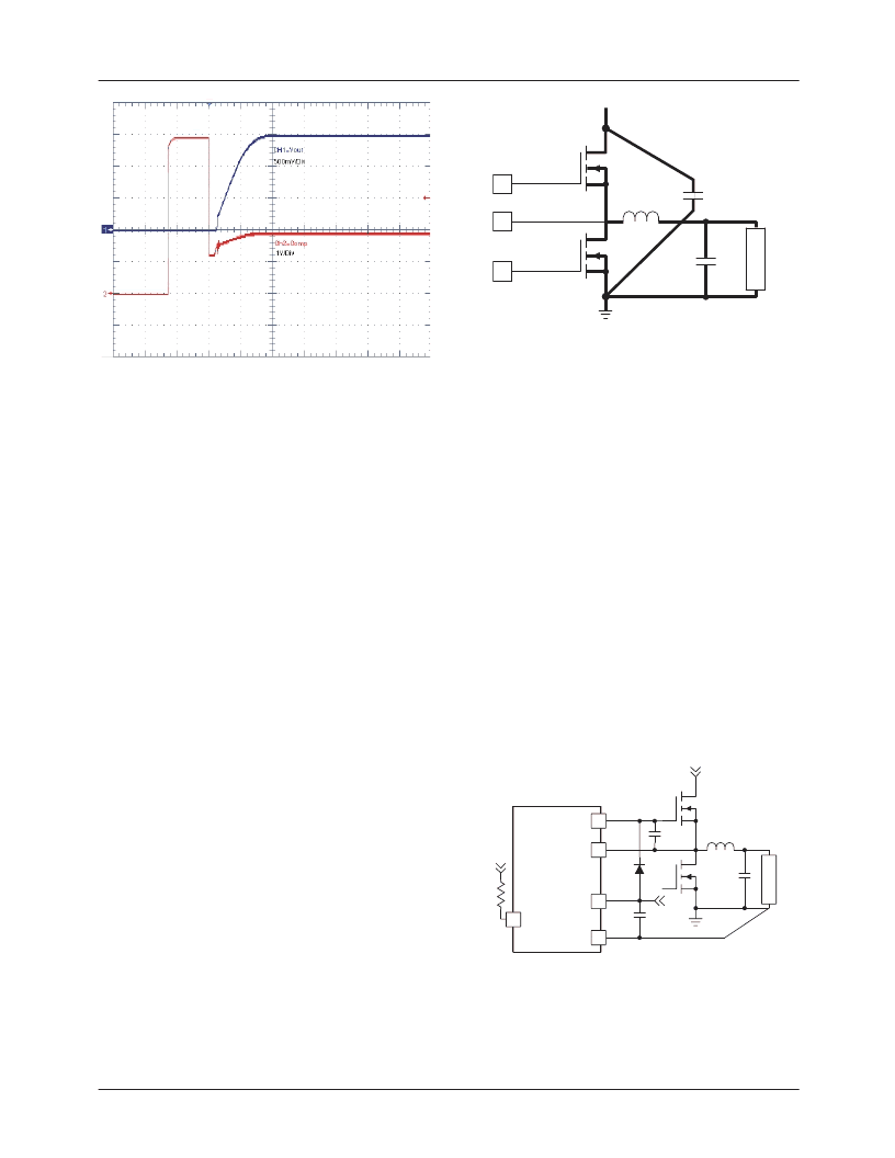
Figure 4. Soft-Start Interval
The FAN6520A incorporates a MOSFET shoot-through
protection method which allows a converter to both sink and
source current. Care should be exercised when designing a
converter with the FAN6520A when it is known that the
converter may sink current.
When the converter is sinking current, it is behaving as a
boost converter that is regulating its input voltage. This
means that the converter is boosting current into the VCC
rail, which supplies the bias voltage to the FAN6520A.
If this current has nowhere to go—such as to other distrib-
uted loads on the VCC rail, through a voltage limiting pro-
tection device, or other methods—the capacitance on the
VCC bus will absorb the current. This situation will allow
the voltage level of the VCC rail to increase. If the voltage
level of the rail is boosted to a level that exceeds the maxi-
mum voltage rating of the FAN6520A, then the IC will expe-
rience an irreversible failure and the converter will no longer
be operational. Ensure that there is a path for the current to
follow other than the capacitance on the rail to prevent this
failure mode.
Application Guidelines
Layout Considerations
As in any high frequency switching converter, layout is very
important. Switching current from one power device to
another can generate voltage transients across the imped-
ances of the interconnecting bond wires and circuit traces.
Use wide, short-printed circuit traces to minimize these
interconnecting impedances. The critical components should
be located as close together as possible, using ground plane
construction or single point grounding.
Figure 5. Printed Circuit Board Power and
Ground Planes or Islands
Figure 5 shows the critical power components of the con-
verter. To minimize the voltage overshoot, the interconnect-
ing wires indicated by heavy lines should be part of a ground
or power plane in a printed circuit board. The components
shown in Figure 5 should be located as close together as
possible. Please note that the capacitors C
IN
and C
OUT
may
each represent numerous physical capacitors. Locate the
FAN6520A within two inches of the Q1 and Q2 MOSFETs.
The circuit traces for the MOSFETs’ gate and source con-
nections from the FAN6520A must be sized to handle up
to 1A peak current.
Figure 5 shows the circuit traces that require additional
layout consideration. Use single point and ground plane
construction for the circuits shown. Minimize any leakage
current paths on the COMP/OCSET pin and locate the
resistor, R
OSCET
close to the COMP/OCSET pin because
the internal current source is only 20μA. Provide local VCC
decoupling between VCC and GND pins. Locate the capaci-
tor, CBOOT as close as practical to the BOOT and PHASE
pins. All components used for feedback compensation
should be located as close to the IC as practical.
Figure 6. PC Board Small Signal Layout Guidelines
+V
OUT
Q2
LDRV
SW
HDRV
Q1
C
IN
L
OUT
C
OUT
L
Vin
FAN
6520A
Q2
VCC
SW
BOOT
Q1
L
OUT
C
OUT
L
GND
C
BOOT
C
VCC
+5V
D
BOOT
COMP/OCSET
+5V
R
O
Vin
相關(guān)PDF資料 |
PDF描述 |
|---|---|
| FAN6520AMX | Single Synchronous Buck PWM Controller |
| FAN6550M | |
| FAN6550MX | |
| FAN6550 | 2A DDR Bus Termination Regulator |
| FAN6555 | 2A DDR Bus Termination Regulator |
相關(guān)代理商/技術(shù)參數(shù) |
參數(shù)描述 |
|---|---|
| FAN6520AM_Q | 功能描述:電壓模式 PWM 控制器 Single Synchronous Buck PWM Controller RoHS:否 制造商:Texas Instruments 輸出端數(shù)量:1 拓?fù)浣Y(jié)構(gòu):Buck 輸出電壓:34 V 輸出電流: 開關(guān)頻率: 工作電源電壓:4.5 V to 5.5 V 電源電流:600 uA 最大工作溫度:+ 125 C 最小工作溫度:- 40 C 封裝 / 箱體:WSON-8 封裝:Reel |
| FAN6520AMX | 功能描述:電壓模式 PWM 控制器 Single Synchronous Buck PWM Controller RoHS:否 制造商:Texas Instruments 輸出端數(shù)量:1 拓?fù)浣Y(jié)構(gòu):Buck 輸出電壓:34 V 輸出電流: 開關(guān)頻率: 工作電源電壓:4.5 V to 5.5 V 電源電流:600 uA 最大工作溫度:+ 125 C 最小工作溫度:- 40 C 封裝 / 箱體:WSON-8 封裝:Reel |
| FAN6520AMX_Q | 功能描述:電壓模式 PWM 控制器 Single Synchronous Buck PWM Controller RoHS:否 制造商:Texas Instruments 輸出端數(shù)量:1 拓?fù)浣Y(jié)構(gòu):Buck 輸出電壓:34 V 輸出電流: 開關(guān)頻率: 工作電源電壓:4.5 V to 5.5 V 電源電流:600 uA 最大工作溫度:+ 125 C 最小工作溫度:- 40 C 封裝 / 箱體:WSON-8 封裝:Reel |
| FAN6520AMXCT | 制造商:Fairchild Semiconductor Corporation 功能描述: |
| FAN6520B | 制造商:FAIRCHILD 制造商全稱:Fairchild Semiconductor 功能描述:Single Synchronous Buck PWM Controller |
發(fā)布緊急采購,3分鐘左右您將得到回復(fù)。