- 您現(xiàn)在的位置:買賣IC網(wǎng) > PDF目錄375715 > FA5314P (FUJI ELECTRIC CO LTD) Bipolar IC For Switching Power Supply Control PDF資料下載
參數(shù)資料
| 型號: | FA5314P |
| 廠商: | FUJI ELECTRIC CO LTD |
| 元件分類: | 穩(wěn)壓器 |
| 英文描述: | Bipolar IC For Switching Power Supply Control |
| 中文描述: | 1.5 A SWITCHING CONTROLLER, 600 kHz SWITCHING FREQ-MAX, PDIP8 |
| 封裝: | DIP-8 |
| 文件頁數(shù): | 11/17頁 |
| 文件大小: | 263K |
| 代理商: | FA5314P |

11
FA531X series
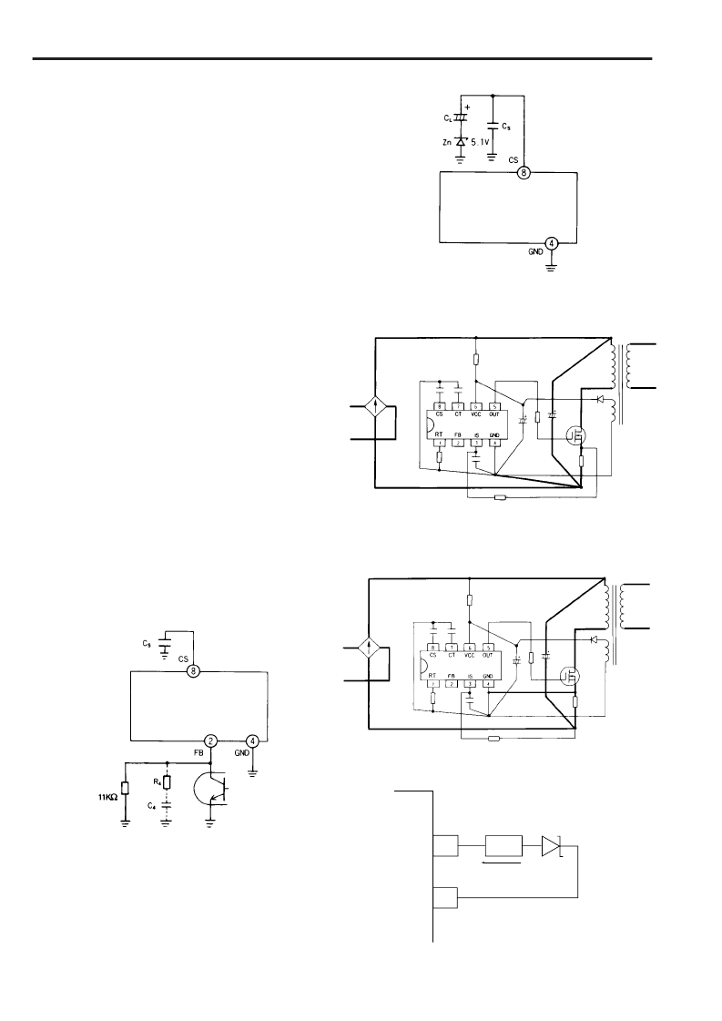
2.Disabling overload shutdown function
As shown in Figure 24, connect a 11k
resistor between the
FB pin and ground. Then, the CS pin voltage does not rise
high enough to reach the reference voltage (7.0V) of the latch
comparator, and the IC does not enter the OFF latch mode.
With this connection, the overvoltage shutdown function is
available.
3.Setting soft start period and OFF latch delay
independently
Figure 25 shows a circuit for setting the soft start period and
OFF latch delay independently. In this circuit, capacitance C
S
determines the soft start period, and capacitance C
L
determines the OFF latch delay. If the overload shutdown and
overvoltage shutdown functions raise the CS pin voltage to
around 5V, zener diode Zn becomes conductive to charge C
L
.
The OFF latch delay can be thus prolonged by C
L
.
4. Laying out V
CC
and ground lines
Figure 26 and 27 show the recommended layouts of V
CC
and
ground lines. The bold lines represent paths carrying large
currents. The lines must have an adequate thickness.
5.Sink current setting for CS terminal
A sink current to CS terminal must be satisfied the following
condition to prevent from the malfunction which uncontrolled
pulse output generates at OUT terminal when latch-mode
protection should be operated for overvoltage.
65
μ
A < Ics(sink) < 500
μ
A at Vcs= 6.5(V)
Ics(sink) : Sink current to CS terminal
Example (for the circuit shown in Fig. 28 )
Ics(sink) = (28(V)–18(V)– 6.5(V) )/7.5(k
)
6
467 (
μ
A) < 500 (
μ
A)
Fig. 24 Disabling overload shutdown function
Fig. 25 Independent setting of soft-start period
and OFF latch delay
Fig. 27 Vcc line and ground line (2) for FA5314/15
Fig. 26 Vcc line and ground line (1) for FA5310B/11B/16/17
Fig. 28 Setting sink current for CS terminal
CS
VCC
7.5k
18V Zener diode
Under 500
μ
A
相關(guān)PDF資料 |
PDF描述 |
|---|---|
| FA5310 | CAPACITOR,SMD 603,100PF,50V,5% |
| FA5310BP | CAP 100PF 50V 5% C0G SMD-0603 BULK SN100 |
| FA5310BPS | CAP 100PF 50V 5% C0G SMD-0603 BULK SN100 |
| FA5311 | CAP 100PF 50V 5% C0G SMD-0603 TR-7-PA SN100 |
| FA5311BP | Bipolar IC For Switching Power Supply Control |
相關(guān)代理商/技術(shù)參數(shù) |
參數(shù)描述 |
|---|---|
| FA5314P(S) | 制造商:未知廠家 制造商全稱:未知廠家 功能描述: |
| FA5314PS | 制造商:FUJI 制造商全稱:Fuji Electric 功能描述:Bipolar IC For Switching Power Supply Control |
| FA5314S | 制造商:未知廠家 制造商全稱:未知廠家 功能描述:Analog IC |
| FA5315P | 制造商:FUJI 制造商全稱:Fuji Electric 功能描述:Bipolar IC For Switching Power Supply Control |
| FA5315P(S) | 制造商:未知廠家 制造商全稱:未知廠家 功能描述: |
發(fā)布緊急采購,3分鐘左右您將得到回復(fù)。