- 您現(xiàn)在的位置:買賣IC網(wǎng) > PDF目錄4343 > EP2AGX95EF35I3N (Altera)IC ARRIA II GX FPGA 95K 1152FBGA PDF資料下載
參數(shù)資料
| 型號: | EP2AGX95EF35I3N |
| 廠商: | Altera |
| 文件頁數(shù): | 2/90頁 |
| 文件大小: | 0K |
| 描述: | IC ARRIA II GX FPGA 95K 1152FBGA |
| 產(chǎn)品培訓(xùn)模塊: | Three Reasons to Use FPGA's in Industrial Designs |
| 標(biāo)準(zhǔn)包裝: | 3 |
| 系列: | Arria II GX |
| LAB/CLB數(shù): | 3747 |
| 邏輯元件/單元數(shù): | 89178 |
| RAM 位總計: | 6839296 |
| 輸入/輸出數(shù): | 452 |
| 電源電壓: | 0.87 V ~ 0.93 V |
| 安裝類型: | 表面貼裝 |
| 工作溫度: | -40°C ~ 100°C |
| 封裝/外殼: | 1152-BBGA |
| 供應(yīng)商設(shè)備封裝: | 1152-FBGA(27x27) |
第1頁當(dāng)前第2頁第3頁第4頁第5頁第6頁第7頁第8頁第9頁第10頁第11頁第12頁第13頁第14頁第15頁第16頁第17頁第18頁第19頁第20頁第21頁第22頁第23頁第24頁第25頁第26頁第27頁第28頁第29頁第30頁第31頁第32頁第33頁第34頁第35頁第36頁第37頁第38頁第39頁第40頁第41頁第42頁第43頁第44頁第45頁第46頁第47頁第48頁第49頁第50頁第51頁第52頁第53頁第54頁第55頁第56頁第57頁第58頁第59頁第60頁第61頁第62頁第63頁第64頁第65頁第66頁第67頁第68頁第69頁第70頁第71頁第72頁第73頁第74頁第75頁第76頁第77頁第78頁第79頁第80頁第81頁第82頁第83頁第84頁第85頁第86頁第87頁第88頁第89頁第90頁
1–2
Chapter 1: Device Datasheet for Arria II Devices
Electrical Characteristics
December 2013
Altera Corporation
damage to the device. Additionally, device operation at the absolute maximum
ratings for extended periods of time may have adverse effects on the device.
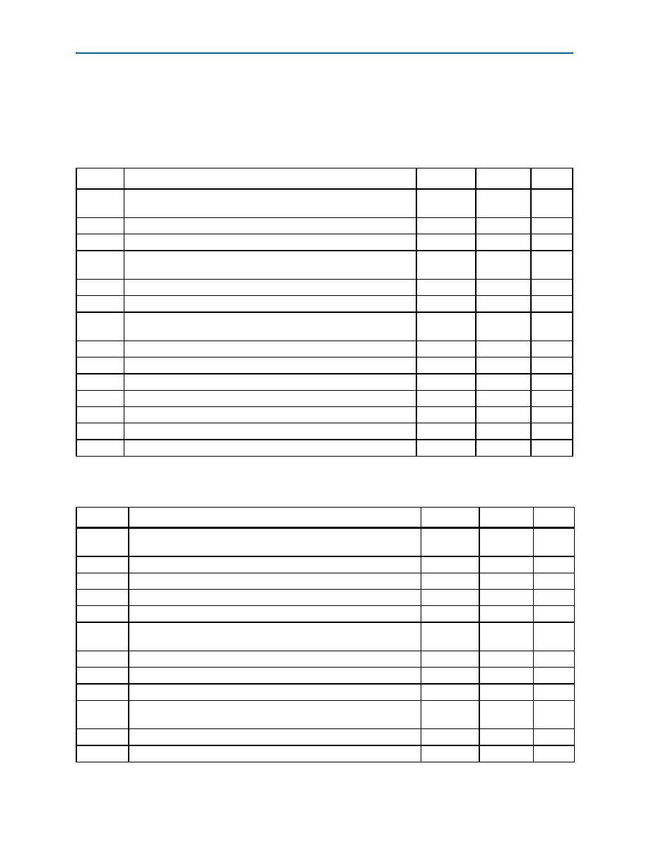
Table 1–1 lists the absolute maximum ratings for Arria II GX devices.
Table 1–2 lists the absolute maximum ratings for Arria II GZ devices.
Table 1–1. Absolute Maximum Ratings for Arria II GX Devices
Symbol
Description
Minimum
Maximum
Unit
VCC
Supplies power to the core, periphery, I/O registers, PCI Express
(PIPE) (PCIe) HIP block, and transceiver PCS
–0.5
1.35
V
VCCCB
Supplies power for the configuration RAM bits
–0.5
1.8
V
VCCBAT
Battery back-up power supply for design security volatile key register
–0.5
3.75
V
VCCPD
Supplies power to the I/O pre-drivers, differential input buffers, and
MSEL circuitry
–0.5
3.75
V
VCCIO
Supplies power to the I/O banks
–0.5
3.9
V
VCCD_PLL
Supplies power to the digital portions of the PLL
–0.5
1.35
V
VCCA_PLL
Supplies power to the analog portions of the PLL and device-wide
power management circuitry
–0.5
3.75
V
VI
DC input voltage
–0.5
4.0
V
IOUT
DC output current, per pin
–25
40
mA
VCCA
Supplies power to the transceiver PMA regulator
—
3.75
V
VCCL_GXB
Supplies power to the transceiver PMA TX, PMA RX, and clocking
—
1.21
V
VCCH_GXB
Supplies power to the transceiver PMA output (TX) buffer
—
1.8
V
TJ
Operating junction temperature
–55
125
°C
TSTG
Storage temperature (no bias)
–65
150
°C
Table 1–2. Absolute Maximum Ratings for Arria II GZ Devices (Part 1 of 2)
Symbol
Description
Minimum
Maximum
Unit
VCC
Supplies power to the core, periphery, I/O registers, PCIe HIP block, and
transceiver PCS
-0.5
1.35
V
VCCCB
Power supply to the configuration RAM bits
-0.5
1.8
V
VCCPGM
Supplies power to the configuration pins
-0.5
3.75
V
VCCAUX
Auxiliary supply
-0.5
3.75
V
VCCBAT
Supplies battery back-up power for design security volatile key register
-0.5
3.75
V
VCCPD
Supplies power to the I/O pre-drivers, differential input buffers, and
MSEL circuitry
-0.5
3.75
V
VCCIO
Supplies power to the I/O banks
-0.5
3.9
V
VCC_CLKIN
Supplies power to the differential clock input
-0.5
3.75
V
VCCD_PLL
Supplies power to the digital portions of the PLL
-0.5
1.35
V
VCCA_PLL
Supplies power to the analog portions of the PLL and device-wide
power management circuitry
-0.5
3.75
V
VI
DC input voltage
-0.5
4.0
V
IOUT
DC output current, per pin
-25
40
mA
相關(guān)PDF資料 |
PDF描述 |
|---|---|
| M24308/2-298 | CONN D-SUB RCPT HD 26P SER 90 |
| GMC65DRXS-S734 | CONN EDGECARD 130PS DIP .100 SLD |
| M24308/2-290 | CONN D-SUB RCPT HD 78P SER 90 |
| FMC13DREI-S734 | CONN EDGECARD 26POS .100 EYELET |
| M24308/4-268 | CONN D-SUB PLUG HD 78P SER 90 |
相關(guān)代理商/技術(shù)參數(shù) |
參數(shù)描述 |
|---|---|
| EP2AGX95EF35I5 | 功能描述:FPGA - 現(xiàn)場可編程門陣列 FPGA - Arria II GX 3747 LABs 452 IOs RoHS:否 制造商:Altera Corporation 系列:Cyclone V E 柵極數(shù)量: 邏輯塊數(shù)量:943 內(nèi)嵌式塊RAM - EBR:1956 kbit 輸入/輸出端數(shù)量:128 最大工作頻率:800 MHz 工作電源電壓:1.1 V 最大工作溫度:+ 70 C 安裝風(fēng)格:SMD/SMT 封裝 / 箱體:FBGA-256 |
| EP2AGX95EF35I5ES | 制造商:Altera Corporation 功能描述:FPGA Arria |
| EP2AGX95EF35I5N | 功能描述:FPGA - 現(xiàn)場可編程門陣列 FPGA - Arria II GX 3747 LABs 452 IOs RoHS:否 制造商:Altera Corporation 系列:Cyclone V E 柵極數(shù)量: 邏輯塊數(shù)量:943 內(nèi)嵌式塊RAM - EBR:1956 kbit 輸入/輸出端數(shù)量:128 最大工作頻率:800 MHz 工作電源電壓:1.1 V 最大工作溫度:+ 70 C 安裝風(fēng)格:SMD/SMT 封裝 / 箱體:FBGA-256 |
| EP2AGXF35NAH | 制造商:Altera Corporation 功能描述: |
| EP2AGZ225FF35C3N | 功能描述:FPGA - 現(xiàn)場可編程門陣列 FPGA - Arria II GZ 8960 LABs 554 IOs RoHS:否 制造商:Altera Corporation 系列:Cyclone V E 柵極數(shù)量: 邏輯塊數(shù)量:943 內(nèi)嵌式塊RAM - EBR:1956 kbit 輸入/輸出端數(shù)量:128 最大工作頻率:800 MHz 工作電源電壓:1.1 V 最大工作溫度:+ 70 C 安裝風(fēng)格:SMD/SMT 封裝 / 箱體:FBGA-256 |
發(fā)布緊急采購,3分鐘左右您將得到回復(fù)。