- 您現(xiàn)在的位置:買賣IC網(wǎng) > PDF目錄4336 > EP2AGX190FF35C5 (Altera)IC ARRIA II GX 190K 1152FBGA PDF資料下載
參數(shù)資料
| 型號: | EP2AGX190FF35C5 |
| 廠商: | Altera |
| 文件頁數(shù): | 14/90頁 |
| 文件大小: | 0K |
| 描述: | IC ARRIA II GX 190K 1152FBGA |
| 產(chǎn)品培訓(xùn)模塊: | Three Reasons to Use FPGA's in Industrial Designs |
| 標(biāo)準(zhǔn)包裝: | 3 |
| 系列: | Arria II GX |
| LAB/CLB數(shù): | 7612 |
| 邏輯元件/單元數(shù): | 181165 |
| RAM 位總計: | 10177536 |
| 輸入/輸出數(shù): | 612 |
| 電源電壓: | 0.87 V ~ 0.93 V |
| 安裝類型: | 表面貼裝 |
| 工作溫度: | 0°C ~ 85°C |
| 封裝/外殼: | 1152-BBGA |
| 供應(yīng)商設(shè)備封裝: | 1152-FBGA(27x27) |
第1頁第2頁第3頁第4頁第5頁第6頁第7頁第8頁第9頁第10頁第11頁第12頁第13頁當(dāng)前第14頁第15頁第16頁第17頁第18頁第19頁第20頁第21頁第22頁第23頁第24頁第25頁第26頁第27頁第28頁第29頁第30頁第31頁第32頁第33頁第34頁第35頁第36頁第37頁第38頁第39頁第40頁第41頁第42頁第43頁第44頁第45頁第46頁第47頁第48頁第49頁第50頁第51頁第52頁第53頁第54頁第55頁第56頁第57頁第58頁第59頁第60頁第61頁第62頁第63頁第64頁第65頁第66頁第67頁第68頁第69頁第70頁第71頁第72頁第73頁第74頁第75頁第76頁第77頁第78頁第79頁第80頁第81頁第82頁第83頁第84頁第85頁第86頁第87頁第88頁第89頁第90頁
Chapter 1: Device Datasheet for Arria II Devices
1–13
Electrical Characteristics
December 2013
Altera Corporation
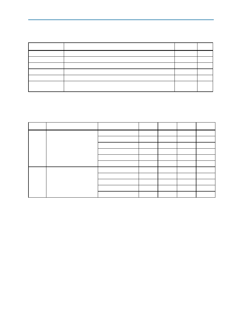
Table 1–17 lists the pin capacitance for Arria II GZ devices.
Internal Weak Pull-Up and Weak Pull-Down Resistors
Table 1–18 lists the weak pull-up and pull-down resistor values for Arria II GX
devices.
Table 1–17. Pin Capacitance for Arria II GZ Devices
Symbol
Description
Typical
Unit
CIOTB
Input capacitance on the top and bottom I/O pins
4
pF
CIOLR
Input capacitance on the left and right I/O pins
4
pF
CCLKTB
Input capacitance on the top and bottom non-dedicated clock input pins
4
pF
CCLKLR
Input capacitance on the left and right non-dedicated clock input pins
4
pF
COUTFB
Input capacitance on the dual-purpose clock output and feedback pins
5
pF
CCLK1, CCLK3, CCLK8,
and CCLK10
Input capacitance for dedicated clock input pins
2
pF
Table 1–18. Internal Weak Pull-up and Weak Pull-Down Resistors for Arria II GX Devices
Symbol
Description
Conditions
Min
Typ
Max
Unit
RPU
Value of I/O pin pull-up resistor
before and during configuration,
as well as user mode if the
programmable pull-up resistor
option is enabled.
725
41
k
728
47
k
835
61
k
10
57
108
k
13
82
163
k
19
143
351
k
RPD
Value of TCK pin pull-down
resistor
VCCIO = 3.3 V ±5%
6
19
29
k
VCCIO = 3.0 V ±5%
6
22
32
k
VCCIO = 2.5 V ±5%
6
25
42
k
VCCIO = 1.8 V ±5%
7
35
70
k
VCCIO = 1.5 V ±5%
8
50
112
k
Notes to Table 1–18:
(1) All I/O pins have an option to enable weak pull-up except configuration, test, and JTAG pins. The weak pull-down feature is only available for
JTAG TCK.
(2) Pin pull-up resistance values may be lower if an external source drives the pin higher than VCCIO.
相關(guān)PDF資料 |
PDF描述 |
|---|---|
| EP2AGX190EF29I5 | IC ARRIA II GX FPGA 190K 780FBGA |
| EP2AGX190EF29C4 | IC ARRIA II GX FPGA 190K 780FBGA |
| APA300-CQ208B | IC FPGA PROASIC+ 300K 208-CQFP |
| A54SX32A-1CQ84 | IC FPGA SX 48K GATES 84-CQFP |
| EP2AGX260FF35C6N | IC ARRIA II GX 260K 1152FBGA |
相關(guān)代理商/技術(shù)參數(shù) |
參數(shù)描述 |
|---|---|
| EP2AGX190FF35C5N | 功能描述:FPGA - 現(xiàn)場可編程門陣列 FPGA - Arria II GX 7612 LABs 612 IOs RoHS:否 制造商:Altera Corporation 系列:Cyclone V E 柵極數(shù)量: 邏輯塊數(shù)量:943 內(nèi)嵌式塊RAM - EBR:1956 kbit 輸入/輸出端數(shù)量:128 最大工作頻率:800 MHz 工作電源電壓:1.1 V 最大工作溫度:+ 70 C 安裝風(fēng)格:SMD/SMT 封裝 / 箱體:FBGA-256 |
| EP2AGX190FF35C6 | 功能描述:FPGA - 現(xiàn)場可編程門陣列 FPGA - Arria II GX 7612 LABs 612 IOs RoHS:否 制造商:Altera Corporation 系列:Cyclone V E 柵極數(shù)量: 邏輯塊數(shù)量:943 內(nèi)嵌式塊RAM - EBR:1956 kbit 輸入/輸出端數(shù)量:128 最大工作頻率:800 MHz 工作電源電壓:1.1 V 最大工作溫度:+ 70 C 安裝風(fēng)格:SMD/SMT 封裝 / 箱體:FBGA-256 |
| EP2AGX190FF35C6N | 功能描述:FPGA - 現(xiàn)場可編程門陣列 FPGA - Arria II GX 7612 LABs 612 IOs RoHS:否 制造商:Altera Corporation 系列:Cyclone V E 柵極數(shù)量: 邏輯塊數(shù)量:943 內(nèi)嵌式塊RAM - EBR:1956 kbit 輸入/輸出端數(shù)量:128 最大工作頻率:800 MHz 工作電源電壓:1.1 V 最大工作溫度:+ 70 C 安裝風(fēng)格:SMD/SMT 封裝 / 箱體:FBGA-256 |
| EP2AGX190FF35C6NGA | 制造商:Altera 功能描述:EP2AGX190FF35C6NGA |
| EP2AGX190FF35I3 | 功能描述:IC ARRIA II GX 190K 1152FBGA RoHS:否 類別:集成電路 (IC) >> 嵌入式 - FPGA(現(xiàn)場可編程門陣列) 系列:Arria II GX 產(chǎn)品變化通告:XC4000(E,L) Discontinuation 01/April/2002 標(biāo)準(zhǔn)包裝:24 系列:XC4000E/X LAB/CLB數(shù):100 邏輯元件/單元數(shù):238 RAM 位總計:3200 輸入/輸出數(shù):80 門數(shù):3000 電源電壓:4.5 V ~ 5.5 V 安裝類型:表面貼裝 工作溫度:-40°C ~ 100°C 封裝/外殼:120-BCBGA 供應(yīng)商設(shè)備封裝:120-CPGA(34.55x34.55) |
發(fā)布緊急采購,3分鐘左右您將得到回復(fù)。