- 您現(xiàn)在的位置:買賣IC網(wǎng) > PDF目錄295886 > EP20K60EFC672-3 (ALTERA CORP) LOADABLE PLD, PBGA672 PDF資料下載
參數(shù)資料
| 型號: | EP20K60EFC672-3 |
| 廠商: | ALTERA CORP |
| 元件分類: | PLD |
| 英文描述: | LOADABLE PLD, PBGA672 |
| 封裝: | 27 X 27 MM, 1 MM PITCH, FINE LINE, BGA-672 |
| 文件頁數(shù): | 26/114頁 |
| 文件大小: | 4116K |
| 代理商: | EP20K60EFC672-3 |
第1頁第2頁第3頁第4頁第5頁第6頁第7頁第8頁第9頁第10頁第11頁第12頁第13頁第14頁第15頁第16頁第17頁第18頁第19頁第20頁第21頁第22頁第23頁第24頁第25頁當(dāng)前第26頁第27頁第28頁第29頁第30頁第31頁第32頁第33頁第34頁第35頁第36頁第37頁第38頁第39頁第40頁第41頁第42頁第43頁第44頁第45頁第46頁第47頁第48頁第49頁第50頁第51頁第52頁第53頁第54頁第55頁第56頁第57頁第58頁第59頁第60頁第61頁第62頁第63頁第64頁第65頁第66頁第67頁第68頁第69頁第70頁第71頁第72頁第73頁第74頁第75頁第76頁第77頁第78頁第79頁第80頁第81頁第82頁第83頁第84頁第85頁第86頁第87頁第88頁第89頁第90頁第91頁第92頁第93頁第94頁第95頁第96頁第97頁第98頁第99頁第100頁第101頁第102頁第103頁第104頁第105頁第106頁第107頁第108頁第109頁第110頁第111頁第112頁第113頁第114頁
IGLOO nano DC and Switching Characteristics
Ad vance v0.2
2-5
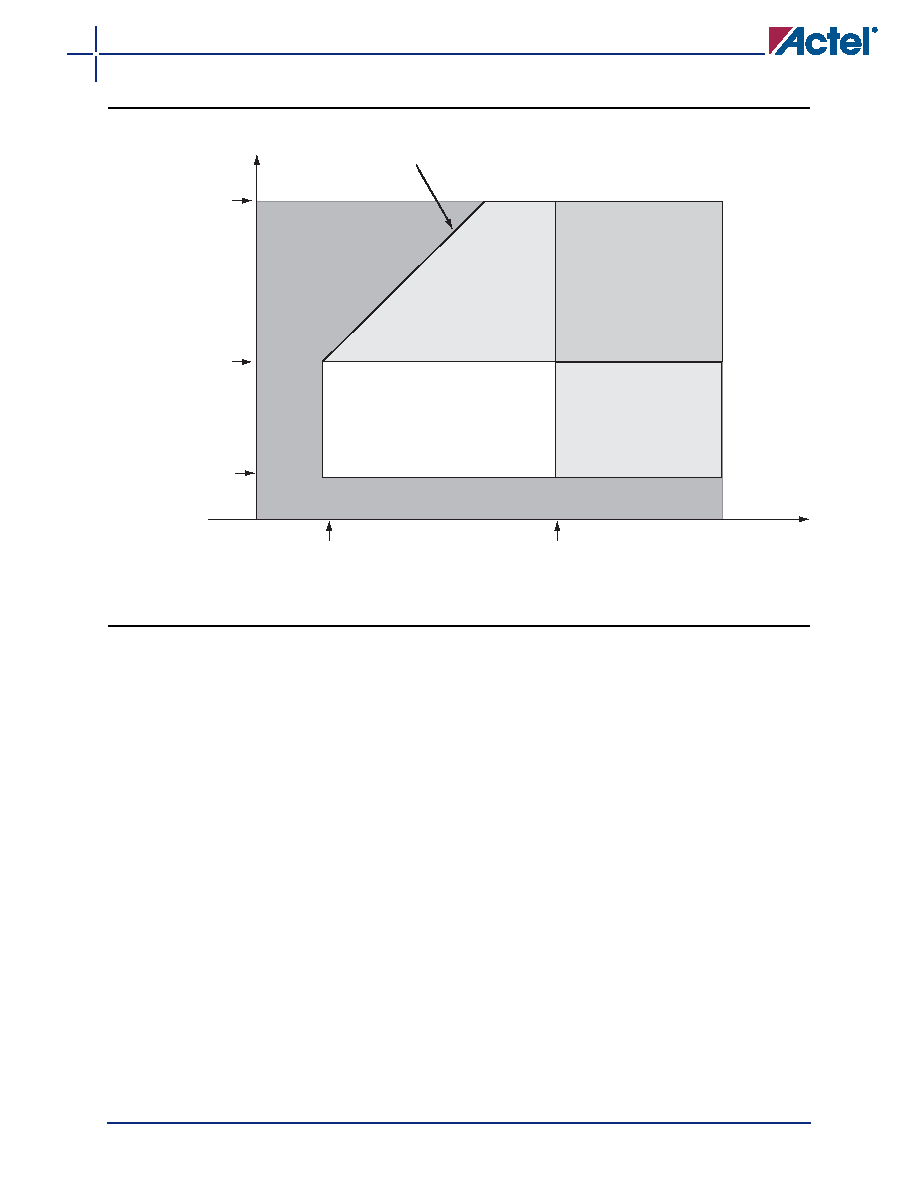
Figure 2-2 V2 Devices – I/O State as a Function of VCCI and VCC Voltage Levels
Region 1: I/O buffers are OFF
Region 2: I/O buffers are ON.
I/Os are functional (except differential inputs)
but slower because V
CCI
/V
CC
are below
specification. For the same reason, input
buffers do not meet V
IH
/V
IL
levels, and
output buffers do not meet V
OH
/V
OL
levels.
Min V
CCI datasheet specification
voltage at a selected I/O
standard; i.e., 1.14 V,1.425 V, 1.7 V,
2.3 V, or 3.0 V
VCC
VCC = 1.14 V
Region 1: I/O Buffers are OFF
Activation trip point:
Va = 0.85 V ± 0.2 V
Deactivation trip point:
Vd = 0.75 V ± 0.2 V
Activation trip point:
Va = 0.9 V ± 0.15 V
Deactivation trip point:
Vd = 0.8 V ± 0.15 V
VCC = 1.575 V
Region 5: I/O buffers are ON
and power supplies are within
specification.
I/Os meet the entire datasheet
and timer specifications for
speed, V
IH
/V
IL
, V
OH
/V
OL
, etc.
Region 4: I/O
buffers are ON.
I/Os are functional
(except differential
but slower because V
CCI is
below specification. For the
same reason, input buffers do not
meet V
IH
/V
IL
levels, and output
buffers do not meet V
OH
/V
OL
levels.
Region 4: I/O
buffers are ON.
I/Os are functional
(except differential inputs)
where VT can be from 0.58 V to 0.9 V (typically 0.75 V)
VCCI
Region 3: I/O buffers are ON.
I/Os are functional; I/O DC
specifications are met,
but I/Os are slower because
the V
CC
is below specification.
V
CC = VCCI + VT
相關(guān)PDF資料 |
PDF描述 |
|---|---|
| EP20K60EFC672 | LOADABLE PLD, PBGA672 |
| EP20K60EQC208 | LOADABLE PLD, PQFP208 |
| EP20K60EQC240 | LOADABLE PLD, PQFP240 |
| EP20K60ERC208 | LOADABLE PLD, PQFP208 |
| EP20K60ERC240 | LOADABLE PLD, PQFP240 |
相關(guān)代理商/技術(shù)參數(shù) |
參數(shù)描述 |
|---|---|
| EP20K60EFI144-1ES | 制造商:未知廠家 制造商全稱:未知廠家 功能描述:FPGA |
| EP20K60EFI144-2ES | 制造商:未知廠家 制造商全稱:未知廠家 功能描述:FPGA |
| EP20K60EFI144-3ES | 制造商:未知廠家 制造商全稱:未知廠家 功能描述:FPGA |
| EP20K60EFI324-1ES | 制造商:未知廠家 制造商全稱:未知廠家 功能描述:FPGA |
| EP20K60EFI324-2ES | 制造商:未知廠家 制造商全稱:未知廠家 功能描述:FPGA |
發(fā)布緊急采購,3分鐘左右您將得到回復(fù)。