- 您現(xiàn)在的位置:買賣IC網(wǎng) > PDF目錄384295 > EM424M3284LBA-7FE (Electronic Theatre Controls, Inc.) 512Mb (4M】4Bank】32) Double DATA RATE SDRAM PDF資料下載
參數(shù)資料
| 型號: | EM424M3284LBA-7FE |
| 廠商: | Electronic Theatre Controls, Inc. |
| 英文描述: | 512Mb (4M】4Bank】32) Double DATA RATE SDRAM |
| 中文描述: | 的512Mb(4分】4Bank】32)的雙倍數(shù)據(jù)速率SDRAM |
| 文件頁數(shù): | 3/20頁 |
| 文件大小: | 343K |
| 代理商: | EM424M3284LBA-7FE |
eorex
EM42AM3284LBA
Jul. 2006
www.eorex.com
3/20
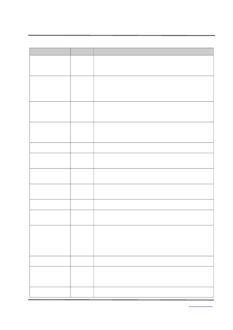
Pin Description (Simplified)
Pin
Name
Function
G2,G3
CLK,/CLK
(System Clock)
Clock input active on the Positive rising edge except for DQ and
DM are active on both edge of the DQS.
CLK and /CLK are differential clock inputs.
(Chip Select)
/CS enables the command decoder when ”L” and disable the
command decoder when “H”.The new command are over-
Looked when the command decoder is disabled but previous
operation will still continue.
(Clock Enable)
Activates the CLK when “H” and deactivates when “L”.
When deactivate the clock,CKE low signifies the power down or
self refresh mode.
(Address)
Row address (A0 to A12) and Calumn address (CA0 to CA8) are
multiplexed on the same pin.
CA10 defines auto precharge at Calumn address.
(Bank Address)
Selects which bank is to be active.
(Row Address Strobe)
Latches Row Addresses on the positive rising edge of the CLK with
/RAS “L”. Enables row access & pre-charge.
(Column Address Strobe)
Latches Column Addresses on the positive rising edge of the CLK
with /CAS low. Enables column access.
(Write Enable)
Latches Column Addresses on the positive rising edge of the CLK
with /CAS low. Enables column access.
(Data Input/Output)
Data Inputs and Outputs are synchronized with both edge of DQS.
(Data Input/Output Mask)
DM controls data inputs.DM0 corresponds to the data on
DQ0~DQ7.DM1 corresponds to the data on DQ8~DQ15……..
H7
/CS
G1
CKE
J8,J9,K7,K9,K1,
K3,J1~J3,H1~H3,
A0~12
H8,H9
BA0, BA1
G9
/RAS
G8
/CAS
G7
/WE
L8,L2,E8,E2
DQS0~3
K8,K2,F8,F2
DM0~3
R8,P7,P8,N7,N8,M7,
M8,L7,L3,M2,M3,N2,
N3,P2,P3,R2,A8,B7,
B8,C7,C8,D7,D8,E7,
E3,D2,D3,C2,C3,B2,
B3,A2
A9,F1,R9/
A1,F9,R1
A7,B1,C9,D1,E9,L9,
M1,N9,P1,R7/A3,B9,
C1,D9,E1,L1,M9,N1,
P9,R3
DQ0~31
(Data Input/Output)
Data inputs and outputs are multiplexed on the same pin.
V
DD
/V
SS
(Power Supply/Ground)
V
DD
and V
SS
are power supply pins for internal circuits.
V
DDQ
/V
SSQ
(Power Supply/Ground)
V
DDQ
and V
SSQ
are power supply pins for the output buffers.
F3,F7
NC/RFU
(No Connection/Reserved for Future Use)
This pin is recommended to be left No Connection on the device.
相關(guān)PDF資料 |
PDF描述 |
|---|---|
| EM424M3284LBA-8FE | 512Mb (4M】4Bank】32) Double DATA RATE SDRAM |
| EM42AM3284LBA | 512Mb (4M】4Bank】32) Double DATA RATE SDRAM |
| EM42AM3284LBA-75F | 512Mb (4M】4Bank】32) Double DATA RATE SDRAM |
| EM42AM3284LBA-75FE | 512Mb (4M】4Bank】32) Double DATA RATE SDRAM |
| EM42AM3284LBA-7FE | 512Mb (4M】4Bank】32) Double DATA RATE SDRAM |
相關(guān)代理商/技術(shù)參數(shù) |
參數(shù)描述 |
|---|---|
| EM424M3284LBA-8FE | 制造商:未知廠家 制造商全稱:未知廠家 功能描述:512Mb (4M×4Bank×32) Double DATA RATE SDRAM |
| EM424M812VTA | 制造商:未知廠家 制造商全稱:未知廠家 功能描述:16Mb ( 2Banks ) Synchronous DRAM |
| EM424M812VTB | 制造商:未知廠家 制造商全稱:未知廠家 功能描述:16Mb ( 2Banks ) Synchronous DRAM |
| EM424M814VTA | 制造商:未知廠家 制造商全稱:未知廠家 功能描述:16Mb ( 2Banks ) Synchronous DRAM |
| EM424M814VTB | 制造商:未知廠家 制造商全稱:未知廠家 功能描述:16Mb ( 2Banks ) Synchronous DRAM |
發(fā)布緊急采購,3分鐘左右您將得到回復(fù)。