- 您現(xiàn)在的位置:買賣IC網(wǎng) > PDF目錄1915 > DS3120N (Maxim Integrated Products)IC FRAMER T1 28-CHANNEL IND PDF資料下載
參數(shù)資料
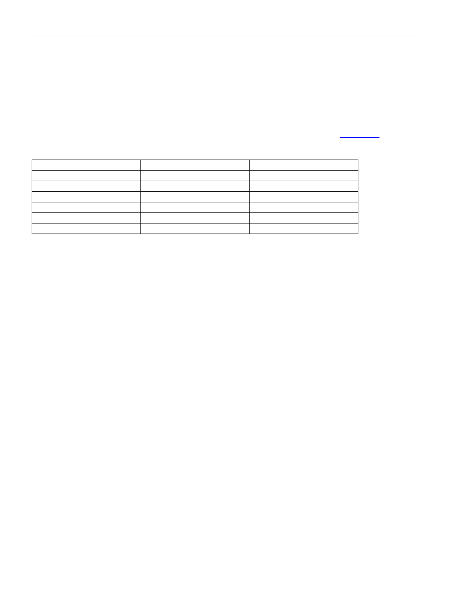
| 型號: | DS3120N |
| 廠商: | Maxim Integrated Products |
| 文件頁數(shù): | 6/133頁 |
| 文件大?。?/td> | 0K |
| 描述: | IC FRAMER T1 28-CHANNEL IND |
| 標準包裝: | 1 |
| 控制器類型: | T1 調(diào)幀器 |
| 接口: | 并行/串行 |
| 電源電壓: | 2.97 V ~ 3.63 V |
| 電流 - 電源: | 300mA |
| 工作溫度: | -40°C ~ 85°C |
| 安裝類型: | 表面貼裝 |
| 封裝/外殼: | 316-BGA |
| 包裝: | 管件 |
第1頁第2頁第3頁第4頁第5頁當前第6頁第7頁第8頁第9頁第10頁第11頁第12頁第13頁第14頁第15頁第16頁第17頁第18頁第19頁第20頁第21頁第22頁第23頁第24頁第25頁第26頁第27頁第28頁第29頁第30頁第31頁第32頁第33頁第34頁第35頁第36頁第37頁第38頁第39頁第40頁第41頁第42頁第43頁第44頁第45頁第46頁第47頁第48頁第49頁第50頁第51頁第52頁第53頁第54頁第55頁第56頁第57頁第58頁第59頁第60頁第61頁第62頁第63頁第64頁第65頁第66頁第67頁第68頁第69頁第70頁第71頁第72頁第73頁第74頁第75頁第76頁第77頁第78頁第79頁第80頁第81頁第82頁第83頁第84頁第85頁第86頁第87頁第88頁第89頁第90頁第91頁第92頁第93頁第94頁第95頁第96頁第97頁第98頁第99頁第100頁第101頁第102頁第103頁第104頁第105頁第106頁第107頁第108頁第109頁第110頁第111頁第112頁第113頁第114頁第115頁第116頁第117頁第118頁第119頁第120頁第121頁第122頁第123頁第124頁第125頁第126頁第127頁第128頁第129頁第130頁第131頁第132頁第133頁
DS3112
103 of 133
11.2
Instruction Register and Instructions
The Instruction register contains a shift register as well as a latched parallel output and is 3 bits in length.
When the TAP controller enters the Shift-IR state, the instruction shift register will be connected between
JTDI and JTDO. While in the Shift-IR state, a rising edge on JTCLK with JTMS low will shift data one
stage towards the serial output at JTDO. A rising edge on JTCLK in the Exit1-IR state or the Exit2-IR
state with JTMS high will move the controller to the Update-IR state. The falling edge of that same
JTCLK will latch the data in the instruction shift register to the instruction parallel output. Instructions
supported by the DS3112 and their respective operational binary codes are shown in
Table 11-1. Instruction Codes
INSTRUCTIONS
SELECTED REGISTER
INSTRUCTION CODES
SAMPLE/PRELOAD
Boundary Scan
010
BYPASS
Bypass
111
EXTEST
Boundary Scan
000
CLAMP
Bypass
011
HIGH-Z
Bypass
100
IDCODE
Device Identification
001
11.2.1 SAMPLE/PRELOAD
A mandatory instruction for the IEEE 1149.1 specification that supports two functions. The digital I/Os of
the DS3112 can be sampled at the Boundary Scan register without interfering with the normal operation
of the device by using the Capture-DR state. SAMPLE/PRELOAD also allows the DS3112 to shift data
into the Boundary Scan register via JTDI using the Shift-DR state.
11.2.2 EXTEST
EXTEST allows testing of all interconnections to the DS3112. When the EXTEST instruction is latched
in the instruction register, the following actions occur. Once enabled via the Update-IR state, the parallel
outputs of all digital output pins will be driven. The Boundary Scan register will be connected between
JTDI and JTDO. The Capture-DR will sample all digital inputs into the Boundary Scan register.
11.2.3 BYPASS
When the BYPASS instruction is latched into the parallel Instruction register, JTDI connects to JTDO
through the one-bit Bypass Test register. This allows data to pass from JTDI to JTDO not affecting the
device's normal operation.
11.2.4 IDCODE
When the IDCODE instruction is latched into the parallel Instruction register, the Identification Test
register is selected. The device identification code will be loaded into the Identification register on the
rising edge of JTCLK following entry into the Capture-DR state. Shift-DR can be used to shift the
identification code out serially via JTDO. During Test-Logic-Reset, the identification code is forced into
the instruction register's parallel output. The device ID code will always have a one in the LSB position.
The next 11 bits identify the manufacturer’s JEDEC number and number of continuation bytes followed
by 16 bits for the device and 4 bits for the version. The device ID code for the DS3112 is 0000B143h.
11.2.5 HIGHZ
All digital outputs will be placed into a high impedance state. The Bypass Register will be connected
between JTDI and JTDO.
相關(guān)PDF資料 |
PDF描述 |
|---|---|
| DS31256+ | IC CTRLR HDLC 256-CHANNEL 256BGA |
| DS3141+ | IC FRAMER DS3/E3 SNGL 144CSBGA |
| DS31412N | IC 12CH DS3/3 FRAMER 349-BGA |
| DS3150TN | IC LIU T3/E3/STS-1 IND 48-TQFP |
| DS3154N+ | IC LIU DS3/E3/STS-1 QD 144CSBGA |
相關(guān)代理商/技術(shù)參數(shù) |
參數(shù)描述 |
|---|---|
| DS3121 | 功能描述:IC TGATOR T1-T3 AGGREGATOR RoHS:否 類別:集成電路 (IC) >> 接口 - 控制器 系列:- 標準包裝:4,900 系列:- 控制器類型:USB 2.0 控制器 接口:串行 電源電壓:3 V ~ 3.6 V 電流 - 電源:135mA 工作溫度:0°C ~ 70°C 安裝類型:表面貼裝 封裝/外殼:36-VFQFN 裸露焊盤 供應商設備封裝:36-QFN(6x6) 包裝:* 其它名稱:Q6396337A |
| DS3121N | 功能描述:IC TGATOR T1-T3 AGGREGATOR IND RoHS:否 類別:集成電路 (IC) >> 接口 - 控制器 系列:- 標準包裝:4,900 系列:- 控制器類型:USB 2.0 控制器 接口:串行 電源電壓:3 V ~ 3.6 V 電流 - 電源:135mA 工作溫度:0°C ~ 70°C 安裝類型:表面貼裝 封裝/外殼:36-VFQFN 裸露焊盤 供應商設備封裝:36-QFN(6x6) 包裝:* 其它名稱:Q6396337A |
| DS31256 | 功能描述:輸入/輸出控制器接口集成電路 256Ch High Thruput HDLC Cntlr RoHS:否 制造商:Silicon Labs 產(chǎn)品: 輸入/輸出端數(shù)量: 工作電源電壓: 最大工作溫度:+ 85 C 最小工作溫度:- 40 C 安裝風格:SMD/SMT 封裝 / 箱體:QFN-64 封裝:Tray |
| DS31256+ | 功能描述:輸入/輸出控制器接口集成電路 256Ch High Thruput HDLC Cntlr RoHS:否 制造商:Silicon Labs 產(chǎn)品: 輸入/輸出端數(shù)量: 工作電源電壓: 最大工作溫度:+ 85 C 最小工作溫度:- 40 C 安裝風格:SMD/SMT 封裝 / 箱體:QFN-64 封裝:Tray |
| DS31256B | 功能描述:輸入/輸出控制器接口集成電路 256Ch High Thruput HDLC Cntlr RoHS:否 制造商:Silicon Labs 產(chǎn)品: 輸入/輸出端數(shù)量: 工作電源電壓: 最大工作溫度:+ 85 C 最小工作溫度:- 40 C 安裝風格:SMD/SMT 封裝 / 箱體:QFN-64 封裝:Tray |
發(fā)布緊急采購,3分鐘左右您將得到回復。