- 您現(xiàn)在的位置:買賣IC網(wǎng) > PDF目錄97868 > DS2151Q (DALLAS SEMICONDUCTOR) DATACOM, FRAMER, PQCC44 PDF資料下載
參數(shù)資料
| 型號: | DS2151Q |
| 廠商: | DALLAS SEMICONDUCTOR |
| 元件分類: | Digital Transmission Controller |
| 英文描述: | DATACOM, FRAMER, PQCC44 |
| 封裝: | PLASTIC, LCC-44 |
| 文件頁數(shù): | 11/47頁 |
| 文件大?。?/td> | 413K |
| 代理商: | DS2151Q |
第1頁第2頁第3頁第4頁第5頁第6頁第7頁第8頁第9頁第10頁當(dāng)前第11頁第12頁第13頁第14頁第15頁第16頁第17頁第18頁第19頁第20頁第21頁第22頁第23頁第24頁第25頁第26頁第27頁第28頁第29頁第30頁第31頁第32頁第33頁第34頁第35頁第36頁第37頁第38頁第39頁第40頁第41頁第42頁第43頁第44頁第45頁第46頁第47頁
MAX1464
Low-Power, Low-Noise Multichannel
Sensor Signal Processor
19
Maxim Integrated
face for programming of instruction code and calibra-
tion coefficients. The MAX1464 serial interface can
operate in 4-wire SPI-compatible mode or in a 3-wire
mode (default on power-up). In 3-wire mode, the DI and
DO lines can be connected together, forming a bidirec-
tional data line. The serial interface lines consist of
chip-select (CS), serial clock (SCLK), data in (DI), and
data out (DO).
The MAX1464 serial interface is selected by asserting
CS low. The serial input clock, SCLK, is gated internally
to begin sequencing the DI input data and outputting
the output data onto DO. When CS rises, the data that
was clocked into DI is loaded into an internal register
set (IRS[7:0]). The MAX1464 chip-select line CS cannot
be connected low continuously for normal operation.
The serial interface can be used both during sensor
calibration, as well as during normal operation. Each
byte of data written into the MAX1464 serial port con-
tains a 4-bit addresses nibble (IRSA [3:0]) and a 4-bit
data nibble (IRSD [3:0]). The IRS register holds both
the IRSD and IRSA nibbles as follows:
IRS [7:0] = IRSD [3:0], IRSA [3:0]
Four bytes of IRS information must be written into the
serial interface to transfer 16 bits of data through IRSD
into a MAX1464 internal register. All serial data written
into the MAX1464 is transferred through the IRS register.
The DI is read in with the LSB of the IRSA nibble first
and the MSB of the IRSD nibble last. Figure 8 shows
serial interface data input.
The IRSA bits are decoded to determine which register
the IRSD bits should be latched into. The IRSA bits
can address the DHR, the PFAR, the CR, and the IMR.
All serial data read from the serial interface is sourced
from the 16-bit DHR. Any data to be read by the serial
interface must first be placed into the internal DHR register
before being accessible for reading by the serial interface.
The entire 16-bit content of the DHR register is read out
through the DO pin by applying 16 successive clock
pulses to SCLK while CS remains low. DHR is clocked
out MSB bit first. Figure 9 shows the 4-wire mode data
read from the DHR register
In 4-wire mode, data is transferred into DI during the
clocking of data out of DO. Therefore, the last 8 bits
clocked into the DI pin during this data transfer are
latched into the IRS register and decoded when CS
returns high.
When the MAX1464 serial interface is configured in 3-
wire mode, the 16-bit DHR data is read out immediately
following the command for 3-wire mode enable. Figure
10 shows the 3-wire enable command (IRS[7:0] = 19h)
clocked into DI with a subsequent 16-bit read of DHR
on DO. DO remains in high impedance (tri-state) until
the 3-wire enable command is received. Then DO goes
into low-impedance drive mode during the next low
cycle of CS. As SCLK is clocked 16 times, the data in
DHR is clocked out at DO. The 3-wire enable command
is the command that sets the MAX1464 ready for output
on DO on the next low cycle of CS. Following the DHR
output on the low cycle of CS, the DO line returns to
high-impedance state until the next 3-wire enable com-
mand is received. The MAX1464 can receive an indefi-
nite number of inputs to DI without the need for a 3-wire
enable command to be received.
When the IRSD[3:0] nibble is written to the command
register (CR), i.e., when IRSA[3:0] = 1000, the nibble is
decoded and a command operation is initiated. The
command register decoding is shown in Table 39.
When the IRSD[3:0] nibble is written to the IMR, i.e.,
when IRSA[3:0] = 1000, the nibble is decoded and a
command operation is initiated. The IMR decoding is
shown in Table 40.
Note that after power is applied and the POR function
completes, the serial interface default is the 3-wire mode
for receiving data on DI only. The DO line is a high-
impedance output until the MAX1464 receives either the
4-wire or 3-wire mode command in the IMR. In the case
of a 3-wire mode command, DO switches from a high-
impedance state to a driving state only for the next cycle
of CS, returning to high impedance afterwards.
All commands, with the exception of programming or
erasing the FLASH memory, are completed within eight
internal master clock cycles of CS returning from low to
high. This is 4s for a 4MHz oscillator frequency or
external clock input (1 internal master clock = 2 exter-
nal/internal oscillator periods). FLASH memory pro-
gramming and erasing require additional time of 80s
and 4.2ms, respectively.
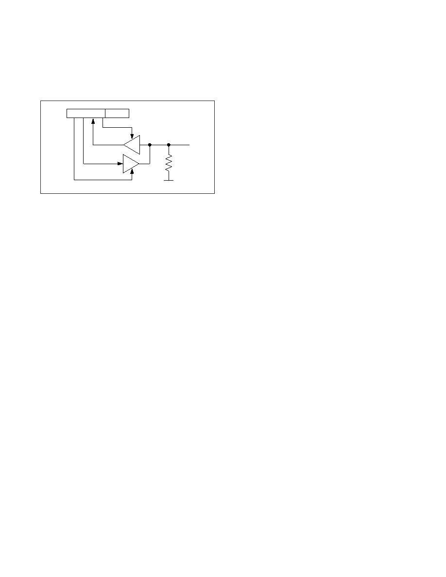
GPIOn
40h OR 41h
GPIOn_Control
EDGE OR LEVEL DETECT
VSS
100k
Ω
TRI-STATE
BUFFER
Figure 7. GPIO1 and GPIO2 Modules
相關(guān)PDF資料 |
PDF描述 |
|---|---|
| DS229S | LINE TRANSCEIVER, PDSO20 |
| DS232AE | LINE TRANSCEIVER, PDSO20 |
| DS232AR | LINE TRANSCEIVER, PDSO16 |
| DS232AR-N | LINE TRANSCEIVER, PDSO16 |
| DS232AS-N | LINE TRANSCEIVER, PDSO16 |
相關(guān)代理商/技術(shù)參數(shù) |
參數(shù)描述 |
|---|---|
| DS2151Q/T&R | 制造商:Maxim Integrated Products 功能描述:IC TXRX T1 1-CHIP 5V LP 44-PLCC |
| DS2151Q/T&R | 功能描述:IC TXRX T1 1-CHIP 5V LP 44-PLCC RoHS:否 類別:集成電路 (IC) >> 接口 - 電信 系列:- 產(chǎn)品培訓(xùn)模塊:Lead (SnPb) Finish for COTS 產(chǎn)品變化通告:Product Discontinuation 06/Feb/2012 標(biāo)準(zhǔn)包裝:750 系列:* |
| DS2151QB | 功能描述:網(wǎng)絡(luò)控制器與處理器 IC RoHS:否 制造商:Micrel 產(chǎn)品:Controller Area Network (CAN) 收發(fā)器數(shù)量: 數(shù)據(jù)速率: 電源電流(最大值):595 mA 最大工作溫度:+ 85 C 安裝風(fēng)格:SMD/SMT 封裝 / 箱體:PBGA-400 封裝:Tray |
| DS2151QB/T&R | 制造商:Maxim Integrated Products 功能描述:T1 SINGLE CHIP XCVR REV B T&R - Tape and Reel |
| DS2151QB/T&R+ | 制造商:Maxim Integrated Products 功能描述:FRAMER DS1/E1/ISDN-PRI/T1 5V 44PLCC - Tape and Reel |
發(fā)布緊急采購,3分鐘左右您將得到回復(fù)。