- 您現(xiàn)在的位置:買賣IC網(wǎng) > PDF目錄376804 > DM96L02N (FAIRCHILD SEMICONDUCTOR CORP) Dual Retriggerable Resettable Monostable Multivibrator PDF資料下載
參數(shù)資料
| 型號: | DM96L02N |
| 廠商: | FAIRCHILD SEMICONDUCTOR CORP |
| 元件分類: | 諧振器 |
| 英文描述: | Dual Retriggerable Resettable Monostable Multivibrator |
| 中文描述: | 96L SERIES, DUAL MONOSTABLE MULTIVIBRATOR, PDIP16 |
| 封裝: | 0.300 INCH, PLASTIC, MS-001, DIP-16 |
| 文件頁數(shù): | 2/6頁 |
| 文件大小: | 68K |
| 代理商: | DM96L02N |
www.fairchildsemi.com
2
D
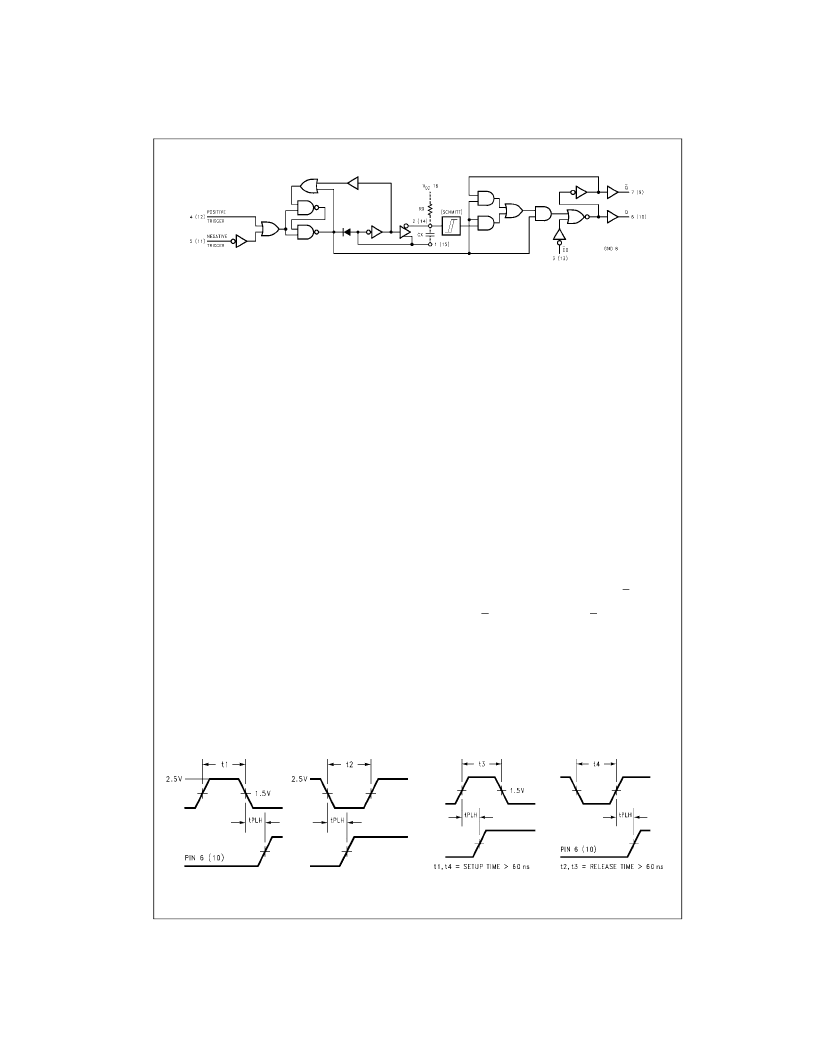
Functional Block Diagram
Operation Notes
1.
TRIGGERING—can be accomplished by a positive-
going transition on pin 4 (12) or a negative-going transi-
tion on pin 5 (11). Triggering begins as a signal crosses
the input V
IL
:V
IH
threshold region; this activates an
internal latch whose unbalanced cross-coupling causes
it to assume a preferred state. As the latch output goes
LOW it disables the gates leading to the Q output and,
through an inverter, turns on the capacitor discharge
transistor. The inverted signal is also fed back to the
latch input to change its state and effectively end the
triggering action; thus the latch and its associated feed-
back perform the function of a differentiator.
The emitters of the latch transistors return to ground
through an enabling transistor which must be turned off
between successive triggers in order for the latch to
proceed through the proper sequence when triggering
is desired. Pin 5 (11) must be HIGH in order to trigger
at pin 4 (12); conversely, pin 4 (12) must be LOW in
order to trigger at pin 5 (11).
2. RETRIGGERING—In a normal cycle, triggering ini-
tiates a rapid discharge of the external timing capacitor,
followed by a ramp voltage run-up at pin 2 (14). The
delay will time out when the ramp voltage reaches the
upper trigger point of a Schmitt circuit, causing the out-
puts to revert to the quiescent state. If another trigger
occurs before the ramp voltage reaches the Schmitt
threshold, the capacitor will be discharged and the
ramp will start again without having disturbed the out-
put. The delay period can therefore be extended for an
arbitrary length of time by insuring that the interval
between triggers is less than the delay time, as deter-
mined by the external capacitor and resistor.
3. NON-RETRIGGERABLE OPERATION—Retriggering
can be inhibited logically, by connecting pin 6 (10) back
to pin 4 (12) or by connecting pin 7 (9) back to pin 5
(11). Either hook-up has the effect of keeping the latch-
enabling transistor turned on during the delay period,
which prevents the input latch from cycling as dis-
cussed above in the section on triggering.
4. OUTPUT PULSE WIDTH—An external resistor R
X
and
an external capacitor C
X
are required, as shown in the
functional block diagram. To minimize stray capaci-
tance and noise pickup, R
X
and C
X
should be located
as close as possible to the circuit. In applications which
require remote trimming of the pulse width, as with a
variable resistor, R
X
should consist of a fixed resistor in
series with the variable resistor; the fixed resistor
should be located as close as possible to the circuit.
The output pulse width t
W
is defined as follows, where
R
X
is in k
, C
X
is in pF and t
W
is in ns.
t
W
=
0.33 R
X
C
X
(1
+
3/R
X
) for C
X
≥
10
3
pF
16 k
≤
R
X
≤
220 k
for 0
°
C to
+
75
°
C
20 k
≤
R
X
≤
100 k
for
55
°
C to
+
125
°
C
C
X
may vary from 0 to any value. For pulse widths with
C
X
less than 10
3
pF see Figure 1.
5. SETUP AND RELEASE TIMES—The setup times
listed below are necessary to allow the latch-enabling
transistor to turn off and the node voltages within the
input latch to stabilize, thus insuring proper cycling of
the latch when the next trigger occurs. The indicated
release times (equivalent to trigger duration) allow time
for the input latch to cycle and its signal to propagate.
6. RESET OPERATION—A LOW signal on C
D
, pin 3
(13), will terminate an output pulse, causing Q to go
LOW and Q to go HIGH. As long as C
D
is held LOW, a
delay period cannot be initiated nor will attempted trig-
gering cause spikes at the outputs. A reset pulse dura-
tion, in the LOW state, of 25 ns is sufficient to insure
resetting. If the reset input goes LOW at the same time
that a trigger transition occurs, the reset will dominate
and the outputs will not respond to the trigger. If the
reset input goes HIGH coincident with a trigger transi-
tion, the circuit will respond to the trigger.
Input to Pin 5 (11)
Pin 4 (12)
=
L
Pin 3 (13)
=
H
Input to Pin 4 (12)
Pins 5 (11) and 3 (13)
=
H
相關PDF資料 |
PDF描述 |
|---|---|
| DM9701F | Gigabit Ethernet PHY Transceiver |
| DM9801A | |
| DM9801E | 1M home Phonrline Network Physical Layer Single Chip Transceiver |
| DMA2271 | Consumer IC |
| DMA2280 | Consumer IC |
相關代理商/技術參數(shù) |
參數(shù)描述 |
|---|---|
| DM96L02N/A+ | 制造商:未知廠家 制造商全稱:未知廠家 功能描述:Monostable Multivibrator |
| DM96LS02 | 制造商:FAIRCHILD 制造商全稱:Fairchild Semiconductor 功能描述:Dual Retriggerable Resettable Monostable Multivibrator |
| DM96LS02M | 功能描述:單穩(wěn)態(tài)多諧振蕩器 Dl Retrig Mo Multivi RoHS:否 制造商:Texas Instruments 每芯片元件:1 邏輯系列:LVC 邏輯類型:Monostable Multivibrator 封裝 / 箱體:SSOP-8 傳播延遲時間:18.6 ns 高電平輸出電流:- 32 mA 低電平輸出電流:32 mA 電源電壓-最大:5.5 V 電源電壓-最小:1.65 V 最大功率耗散: 最大工作溫度:+ 85 C 最小工作溫度:- 40 C 封裝:Reel |
| DM96LS02MX | 功能描述:單穩(wěn)態(tài)多諧振蕩器 Dl Retrig Mo Multivi RoHS:否 制造商:Texas Instruments 每芯片元件:1 邏輯系列:LVC 邏輯類型:Monostable Multivibrator 封裝 / 箱體:SSOP-8 傳播延遲時間:18.6 ns 高電平輸出電流:- 32 mA 低電平輸出電流:32 mA 電源電壓-最大:5.5 V 電源電壓-最小:1.65 V 最大功率耗散: 最大工作溫度:+ 85 C 最小工作溫度:- 40 C 封裝:Reel |
| DM96LS02N | 功能描述:單穩(wěn)態(tài)多諧振蕩器 Dl Retrig Mo Multivi RoHS:否 制造商:Texas Instruments 每芯片元件:1 邏輯系列:LVC 邏輯類型:Monostable Multivibrator 封裝 / 箱體:SSOP-8 傳播延遲時間:18.6 ns 高電平輸出電流:- 32 mA 低電平輸出電流:32 mA 電源電壓-最大:5.5 V 電源電壓-最小:1.65 V 最大功率耗散: 最大工作溫度:+ 85 C 最小工作溫度:- 40 C 封裝:Reel |
發(fā)布緊急采購,3分鐘左右您將得到回復。