- 您現(xiàn)在的位置:買賣IC網(wǎng) > PDF目錄376777 > DM6806 (Electronic Theatre Controls, Inc.) DM5806 DATA MODULE DIGITAL I/O BOARD PDF資料下載
參數(shù)資料
| 型號(hào): | DM6806 |
| 廠商: | Electronic Theatre Controls, Inc. |
| 英文描述: | DM5806 DATA MODULE DIGITAL I/O BOARD |
| 中文描述: | DM5806數(shù)據(jù)模塊數(shù)字I / O板 |
| 文件頁數(shù): | 17/64頁 |
| 文件大?。?/td> | 270K |
| 代理商: | DM6806 |
第1頁第2頁第3頁第4頁第5頁第6頁第7頁第8頁第9頁第10頁第11頁第12頁第13頁第14頁第15頁第16頁當(dāng)前第17頁第18頁第19頁第20頁第21頁第22頁第23頁第24頁第25頁第26頁第27頁第28頁第29頁第30頁第31頁第32頁第33頁第34頁第35頁第36頁第37頁第38頁第39頁第40頁第41頁第42頁第43頁第44頁第45頁第46頁第47頁第48頁第49頁第50頁第51頁第52頁第53頁第54頁第55頁第56頁第57頁第58頁第59頁第60頁第61頁第62頁第63頁第64頁
1-5
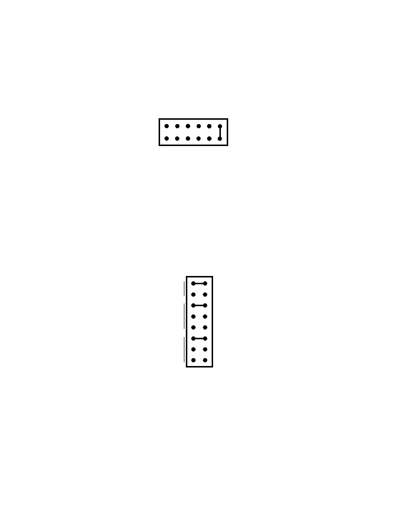
P4 — Interrupt Source Select (Factory Setting: EXT)
This header connector, shown in Figure 1-4, lets you connect one of six interrupt sources for interrupt genera-
tion. These sources are: OT0, OT1, and OT2, which are the three 8254 timer/counter outputs; PC3, which is the
INTRA signal from the 8255 PPI; PC0, which is the INTRB signal from the 8255 PPI; and EXT, an external
interrupt you can route onto the board through the P2 I/O connector. To connect an interrupt source, place the
jumper across the desired set of pins. Note that only ONE interrupt source can be activated at a time.
Fig. 1-4 — Interrupt Source Select Jumper, P4
E
P
P
O
O
O
P4
P5 — 8254 Timer/Counter Clock Sources (Factory Settings: CLK0-OSC, CLK1-OT0, CLK2-OT1)
This header connector, shown in Figure 1-5, lets you select the clock sources for the 8254 timer/counters, TC0,
TC1, and TC2. The factory setting cascades all three timer/counters, with the clock source for TC0 being the on-
board 8 MHz oscillator, the output of TC0 providing the clock for TC1, and the output of TC1 providing the clock
for TC2. You can connect any or all of the sources to an external clock input through the P6 on-board I/O connector,
or you can set TC1 and TC2 to be clocked by the 8 MHz oscillator. Figure 1-6 shows a block diagram of the timer/
counter circuitry to help you with these connections.
NOTE:
When installing jumpers on this header, make sure that only one jumper is installed in each group of
two or three CLK pins.
OSC
EC0
OT0
OSC
EC1
OT1
OSC
EC2
Fig. 1-5 — 8254 Timer/Counter Clock Source Jumpers, P5
P5
C
C
C
相關(guān)PDF資料 |
PDF描述 |
|---|---|
| DM6380L | V.34 Integrated Data/ Fax/Voice/Speakerphone Modem Device Set |
| DM6381F | V.34 Integrated Data/ Fax/Voice/Speakerphone Modem Device Set |
| DM6382F | V.34 Integrated Data/ Fax/Voice/Speakerphone Modem Device Set |
| DM6383F | V.34 Integrated Data/ Fax/Voice/Speakerphone Modem Device Set |
| DM336P | V.34 Integrated Data/ Fax/Voice/Speakerphone Modem Device Set |
相關(guān)代理商/技術(shù)參數(shù) |
參數(shù)描述 |
|---|---|
| DM6CD330J03 | 制造商:n/a 功能描述:DM6X033 S7B3A |
| DM6-M25 | 制造商:Mencom 功能描述: |
| DM6-MF-25 | 制造商:Mencom 功能描述: |
| DM6-MM-06 | 制造商:Mencom 功能描述: |
| DM6-MM-10 | 制造商:Mencom 功能描述: |
發(fā)布緊急采購,3分鐘左右您將得到回復(fù)。