- 您現(xiàn)在的位置:買賣IC網 > PDF目錄376698 > DFC10E48S3.3 SINGLE OUTPUT PDF資料下載
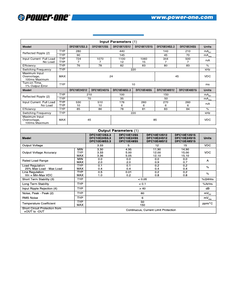
參數(shù)資料
| 型號: | DFC10E48S3.3 |
| 英文描述: | SINGLE OUTPUT |
| 中文描述: | 單輸出 |
| 文件頁數(shù): | 2/3頁 |
| 文件大小: | 1075K |
| 代理商: | DFC10E48S3.3 |

2
DFC10 SERIES – SINGLE OUTPUT
NOTES
(1)
All parameters measured at Tc = 25°C, nominal input voltage and full rated load unless otherwise noted.
Refer to the Technical Reference Section for the definition of terms, measurement circuits and other
information.
Noise is measured per Technical Reference Section. Measurement bandwidth is 0-20 MHz for peak-peak
measurements, 10 kHz to 1 MHz for RMS measurements. Output noise is measured with a 0.01μF /
100V ceramic capacitor in parallel with a 1μf / 35V Tantalum capacitor, 1 inch from the output pins to
simulate standard PCB decoupling capacitance.
Short term stability is specified after a 30 minute warmup at full load, constant line and recording the
drift over a 24 hour period.
The input ripple rejection is specified for DC to 120 Hz ripple with a modulation amplitude of 1% of Vin.
(2)
(3)
(4)
DFC10 SERIES APPLICATION NOTES:
External Capacitance Requirements
No external capacitance is required for operation of the DFC10
Series. If a capacitive input source is farther than 1” from the
converter, an additional capacitor may be required at the input pins
for proper operation. This input capacitor should have an ESR
greater than 0.25 ohms. Input capacitors with an ESR less than 0.25
ohms may cause peaking of the input filter and actually degrade
circuit performance.
External output capacitance is not required for operation, however it
is recommended that 1 F to 10 F of tantalum and 0.001 to 0.1 F
ceramic capacitance be selected for reduced system noise. Additional
output capacitance may be added for increased filtering, but should
not exceed 400 F.
Negative Outputs
A negative output voltage may be obtained by connecting the +OUT
to circuit ground and connecting -OUT as the negative output.
相關PDF資料 |
PDF描述 |
|---|---|
| DFC10E12S3.3 | SINGLE OUTPUT |
| DFC10E48S12 | SINGLE OUTPUT |
| DFC10E48S15 | SINGLE OUTPUT |
| DFC10E48S5 | SINGLE OUTPUT |
| DFC10E12S12 | DIODE LASER 5MW 1550NM TO-18 |
相關代理商/技術參數(shù) |
參數(shù)描述 |
|---|---|
| DFC10E48S5 | 功能描述:DC/DC轉換器 72-5Vin 2000mA 5Vout 11W RoHS:否 制造商:Murata 產品: 輸出功率: 輸入電壓范圍:3.6 V to 5.5 V 輸入電壓(標稱): 輸出端數(shù)量:1 輸出電壓(通道 1):3.3 V 輸出電流(通道 1):600 mA 輸出電壓(通道 2): 輸出電流(通道 2): 安裝風格:SMD/SMT 封裝 / 箱體尺寸: |
| DFC10E48S5 RPL | 制造商:Power-One 功能描述:POWER SUPPLY - Bulk |
| DFC10E48S5S213 | 制造商:Power-One 功能描述: |
| DFC10S205BASE | 制造商:Power-One 功能描述: |
| DFC10S219 | 制造商:Power-One 功能描述: |
發(fā)布緊急采購,3分鐘左右您將得到回復。