- 您現(xiàn)在的位置:買賣IC網(wǎng) > PDF目錄1992 > CYW173SXC (Silicon Laboratories Inc)IC CLK GEN TAPE DRV 4CH 16SOIC PDF資料下載
參數(shù)資料
| 型號: | CYW173SXC |
| 廠商: | Silicon Laboratories Inc |
| 文件頁數(shù): | 4/5頁 |
| 文件大?。?/td> | 0K |
| 描述: | IC CLK GEN TAPE DRV 4CH 16SOIC |
| 標(biāo)準(zhǔn)包裝: | 48 |
| 類型: | 時鐘/頻率發(fā)生器 |
| PLL: | 是 |
| 主要目的: | CPB Tape Drive System |
| 輸入: | 晶體 |
| 輸出: | TTL |
| 電路數(shù): | 1 |
| 比率 - 輸入:輸出: | 1:4 |
| 差分 - 輸入:輸出: | 無/無 |
| 頻率 - 最大: | 100MHz |
| 電源電壓: | 3.135 V ~ 3.465 V |
| 工作溫度: | 0°C ~ 70°C |
| 安裝類型: | * |
| 封裝/外殼: | * |
| 供應(yīng)商設(shè)備封裝: | * |
| 包裝: | * |
W173
......... Document #: 38-07313 Rev. *B Page Page 4 of 5 of 5
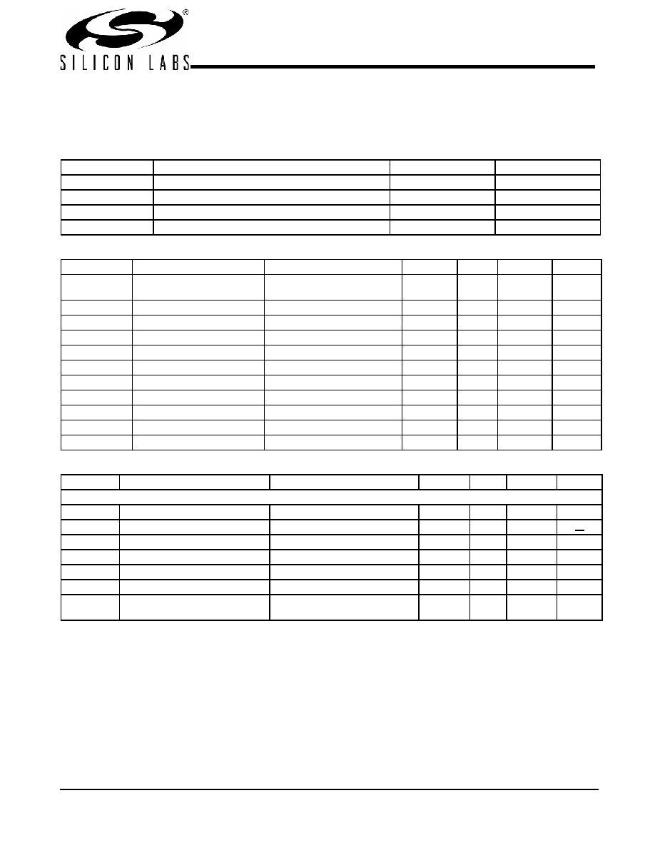
Absolute Maximum Ratings[2]
Stresses greater than those listed in this table may cause
permanent damage to the device. These represent a stress
rating only. Operation of the device at these or any other condi-
tions above those specified in the operating sections of this
specification is not implied. Maximum conditions for extended
periods may affect reliability.
Table 1:
Parameter
Description
Rating
Unit
VDD, VIN
Voltage on Any Pin with Respect to GND
–0.5 to +7.0
V
TSTG
Storage Temperature
–65 to +150
°C
TB
Ambient Temperature under Bias
–55 to +125
°C
TA
Operating Temperature
0 to +70
°C
DC Electrical Characteristics: TA = 0°C to +70°C, VDD = 3.3V±5%
Parameter
Description
Test Condition
Min.
Typ.
Max.
Unit
IDD
Supply Current
Note: CLK output = 50.0 MHz
output loaded
40
mA
VIL
Input Low Voltage
VCC = 5.0V
0.8
V
VIH
Input High Voltage
VCC = 5.0V
2.0
V
VOL
Output Low Voltage
IOL = 1 mA
50
mV
VOH
Output High Voltage
IOH = –1 mA
3.1
V
IIL
Input Low Current
10
A
IIH
Input High Current
10
A
RP
Input Pull-up Resistor
VIN = 0V
500
k
CI
Input Capacitance
Except X1 and X2
6
pF
LI
Input Inductance
Except X1 and X2
7
nH
CL
XTAL Load Capacitance
Total load to crystal
12
pF
AC Electrical Characteristics: TA = 0°C to +70°C, VCC = 3.3V±5%
Parameter
Description
Test Condition
Min.
Typ.
Max.
Unit
Clock Outputs
tJC
Output Clock Jitter, Cycle-to-Cycle Excluding 13.2-MHz output
±175
±250
ps
ZO
Output Buffer Impedance
40
W
dT
Output Duty Cycle
45
50
55
%
tR
Rise Time
Between 0.4V and 2.4V
0.8
1.5
4.0
V/ns
tF
Fall Time
Between 2.4V and 0.4V
0.8
1.5
4.0
V/ns
tPU
Stabilization Time from Power-Up To within 0.1% of final frequency
1.5
3.0
ms
fA
Long Term Output Frequency
Stability
Over VCC and TA range
0.01
%
Note:
2. Multiple Supplies: The Voltage on any input or I/O pin cannot exceed the power pin during power-up. Power supply sequencing is NOT required.
3. All AC tests are performed using the circuit shown in Figure 1 to simulate typical system load conditions. Measurements are taken at the load. Threshold voltage
for timing measurements is 1.5V.
相關(guān)PDF資料 |
PDF描述 |
|---|---|
| CYW305OXC | IC CLOCK W305 SOLANO 56SSOP |
| DAC5674IPHPG4 | IC DAC 14BIT 400MSPS 48-HTQFP |
| DAC7621EBG4 | IC SNGL 12BIT PARALLEL D/A 20SSO |
| DAC7801KPG4 | IC DUAL 12BIT CMOS DAC 24-DIP |
| DAC8043AESZ | IC DAC 12BIT MULT SRL INP 8SOIC |
相關(guān)代理商/技術(shù)參數(shù) |
參數(shù)描述 |
|---|---|
| CYW173SXCT | 功能描述:時鐘發(fā)生器及支持產(chǎn)品 Tape Media Backup Dr Clk Gen W173 DS RoHS:否 制造商:Silicon Labs 類型:Clock Generators 最大輸入頻率:14.318 MHz 最大輸出頻率:166 MHz 輸出端數(shù)量:16 占空比 - 最大:55 % 工作電源電壓:3.3 V 工作電源電流:1 mA 最大工作溫度:+ 85 C 安裝風(fēng)格:SMD/SMT 封裝 / 箱體:QFN-56 |
| CYW180-01SX | 制造商:CYPRESS 制造商全稱:Cypress Semiconductor 功能描述:Peak Reducing EMI Solution |
| CYW180-01SXT | 制造商:CYPRESS 制造商全稱:Cypress Semiconductor 功能描述:Peak Reducing EMI Solution |
| CYW180-02SX | 制造商:CYPRESS 制造商全稱:Cypress Semiconductor 功能描述:Peak Reducing EMI Solution |
| CYW180-02SXT | 制造商:CYPRESS 制造商全稱:Cypress Semiconductor 功能描述:Peak Reducing EMI Solution |
發(fā)布緊急采購,3分鐘左右您將得到回復(fù)。