- 您現(xiàn)在的位置:買賣IC網(wǎng) > PDF目錄295376 > CY7C1472BV25-250BZXI (CYPRESS SEMICONDUCTOR CORP) 4M X 18 ZBT SRAM, 3 ns, PBGA165 PDF資料下載
參數(shù)資料
| 型號: | CY7C1472BV25-250BZXI |
| 廠商: | CYPRESS SEMICONDUCTOR CORP |
| 元件分類: | SRAM |
| 英文描述: | 4M X 18 ZBT SRAM, 3 ns, PBGA165 |
| 封裝: | 15 X 17 MM, 1.40 MM HEIGHT, LEAD FREE, FBGA-165 |
| 文件頁數(shù): | 4/29頁 |
| 文件大?。?/td> | 884K |
| 代理商: | CY7C1472BV25-250BZXI |
第1頁第2頁第3頁當(dāng)前第4頁第5頁第6頁第7頁第8頁第9頁第10頁第11頁第12頁第13頁第14頁第15頁第16頁第17頁第18頁第19頁第20頁第21頁第22頁第23頁第24頁第25頁第26頁第27頁第28頁第29頁
CY7C1470BV25
CY7C1472BV25, CY7C1474BV25
Document #: 001-15032 Rev. *D
Page 12 of 29
IEEE 1149.1 Serial Boundary Scan (JTAG)
The CY7C1470BV25, CY7C1472BV25, and CY7C1474BV25
incorporates a serial boundary scan test access port (TAP). This
port operates in accordance with IEEE Standard 1149.1-1990
but does not have the set of functions required for full 1149.1
compliance. These functions from the IEEE specification are
excluded because their inclusion places an added delay in the
critical speed path of the SRAM. Note that the TAP controller
functions in a manner that does not conflict with the operation of
other devices using 1149.1 fully compliant TAPs. The TAP
operates using JEDEC-standard 2.5V IO logic levels.
The CY7C1470BV25, CY7C1472BV25, and CY7C1474BV25
contains a TAP controller, instruction register, boundary scan
register, bypass register, and ID register.
Disabling the JTAG Feature
It is possible to operate the SRAM without using the JTAG
feature. To disable the TAP controller, TCK must be tied LOW
(VSS) to prevent clocking of the device. TDI and TMS are inter-
nally pulled up and may be unconnected. They may alternately
be connected to VDD through a pull up resistor. TDO must be left
unconnected. During power up, the device comes up in a reset
state, which does not interfere with the operation of the device.
The 0/1 next to each state represents the value of TMS at the
rising edge of TCK.
Test Access Port (TAP)
Test Clock (TCK)
The test clock is used only with the TAP controller. All inputs are
captured on the rising edge of TCK. All outputs are driven from
the falling edge of TCK.
Test MODE SELECT (TMS)
The TMS input is used to give commands to the TAP controller
and is sampled on the rising edge of TCK. It is allowable to leave
this ball unconnected if the TAP is not used. The ball is pulled up
internally, resulting in a logic HIGH level.
Test Data-In (TDI)
The TDI ball is used to serially input information into the registers
and can be connected to the input of any of the registers. The
register between TDI and TDO is chosen by the instruction that
is loaded into the TAP instruction register. For information about
loading the instruction register, see the TAP Controller State
Diagram. TDI is internally pulled up and can be unconnected if
the TAP is unused in an application. TDI is connected to the most
significant bit (MSB) of any register. (See TAP Controller Block
Diagram.)
Test Data-Out (TDO)
The TDO output ball is used to serially clock data-out from the
registers. The output is active depending upon the current state
of the TAP state machine. The output changes on the falling edge
of TCK. TDO is connected to the least significant bit (LSB) of any
register. (See TAP Controller State Diagram.)
Performing a TAP Reset
A RESET is performed by forcing TMS HIGH (VDD) for five rising
edges of TCK. This RESET does not affect the operation of the
SRAM and may be performed while the SRAM is operating.
During power up, the TAP is reset internally to ensure that TDO
comes up in a High-Z state.
TAP Registers
Registers are connected between the TDI and TDO balls to scan
the data in and out of the SRAM test circuitry. Only one register
can be selected at a time through the instruction register. Data is
serially loaded into the TDI ball on the rising edge of TCK. Data
is output on the TDO ball on the falling edge of TCK.
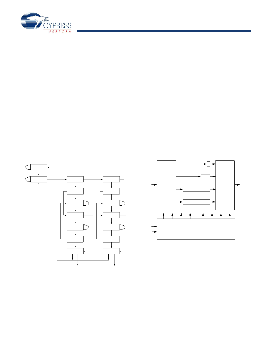
Figure 2. TAP Controller State Diagram
TEST-LOGIC
RESET
RUN-TEST/
IDLE
SELECT
DR-SCA N
SELECT
IR-SCA N
CA PTURE-DR
SHIFT-DR
CA PTURE-IR
SHIFT-IR
EXIT1-DR
PA USE-DR
EXIT1-IR
PA USE-IR
EXIT2-DR
UPDA TE-DR
EXIT2-IR
UPDA TE-IR
1
0
1
0
1
0
1
0
1
0
1
0
1
0
Figure 3. TAP Controller Block Diagram
Bypass Register
0
Instruction Register
0
1
2
Identification Register
0
1
2
29
30
31
.
Boundary Scan Register
0
1
2
.
x
.
Selection
Circuitry
TCK
TM S
TAP CONTROLLER
TDI
TDO
Selection
Circuitry
相關(guān)PDF資料 |
PDF描述 |
|---|---|
| CY7C164-15PC | 16K x 4 Static RAM |
| CY7C164-25PC | 16K x 4 Static RAM |
| CY7C164-15VC | 16K x 4 Static RAM |
| CY7C164-20PC | 16K x 4 Static RAM |
| CY7C164-20VC | 16K x 4 Static RAM |
相關(guān)代理商/技術(shù)參數(shù) |
參數(shù)描述 |
|---|---|
| CY7C1472BV33-167AXI | 功能描述:靜態(tài)隨機(jī)存取存儲器 72MB (4Mx18) 3.3v 167MHz 靜態(tài)隨機(jī)存取存儲器 RoHS:否 制造商:Cypress Semiconductor 存儲容量:16 Mbit 組織:1 M x 16 訪問時間:55 ns 電源電壓-最大:3.6 V 電源電壓-最小:2.2 V 最大工作電流:22 uA 最大工作溫度:+ 85 C 最小工作溫度:- 40 C 安裝風(fēng)格:SMD/SMT 封裝 / 箱體:TSOP-48 封裝:Tray |
| CY7C1472BV33-167BZC | 功能描述:靜態(tài)隨機(jī)存取存儲器 4Mx18,3.3V NoBL PL 靜態(tài)隨機(jī)存取存儲器 RoHS:否 制造商:Cypress Semiconductor 存儲容量:16 Mbit 組織:1 M x 16 訪問時間:55 ns 電源電壓-最大:3.6 V 電源電壓-最小:2.2 V 最大工作電流:22 uA 最大工作溫度:+ 85 C 最小工作溫度:- 40 C 安裝風(fēng)格:SMD/SMT 封裝 / 箱體:TSOP-48 封裝:Tray |
| CY7C1472BV33-167BZCT | 功能描述:靜態(tài)隨機(jī)存取存儲器 4Mx18,3.3V NoBL PL 靜態(tài)隨機(jī)存取存儲器 RoHS:否 制造商:Cypress Semiconductor 存儲容量:16 Mbit 組織:1 M x 16 訪問時間:55 ns 電源電壓-最大:3.6 V 電源電壓-最小:2.2 V 最大工作電流:22 uA 最大工作溫度:+ 85 C 最小工作溫度:- 40 C 安裝風(fēng)格:SMD/SMT 封裝 / 箱體:TSOP-48 封裝:Tray |
| CY7C1472BV33-167ZXI | 制造商:Rochester Electronics LLC 功能描述: 制造商:Cypress Semiconductor 功能描述: |
| CY7C1472BV33-200AXC | 功能描述:靜態(tài)隨機(jī)存取存儲器 4Mx18,3.3V NoBL PL 靜態(tài)隨機(jī)存取存儲器 RoHS:否 制造商:Cypress Semiconductor 存儲容量:16 Mbit 組織:1 M x 16 訪問時間:55 ns 電源電壓-最大:3.6 V 電源電壓-最小:2.2 V 最大工作電流:22 uA 最大工作溫度:+ 85 C 最小工作溫度:- 40 C 安裝風(fēng)格:SMD/SMT 封裝 / 箱體:TSOP-48 封裝:Tray |
發(fā)布緊急采購,3分鐘左右您將得到回復(fù)。