- 您現(xiàn)在的位置:買賣IC網(wǎng) > PDF目錄9005 > CY28409ZXC (Silicon Laboratories Inc)IC CLOCK CK409GRANTSDALE 56TSSOP PDF資料下載
參數(shù)資料
| 型號: | CY28409ZXC |
| 廠商: | Silicon Laboratories Inc |
| 文件頁數(shù): | 12/16頁 |
| 文件大?。?/td> | 0K |
| 描述: | IC CLOCK CK409GRANTSDALE 56TSSOP |
| 標(biāo)準(zhǔn)包裝: | 35 |
| 類型: | * |
| PLL: | 是 |
| 輸入: | 晶體 |
| 輸出: | 時鐘 |
| 電路數(shù): | 1 |
| 比率 - 輸入:輸出: | 1:21 |
| 差分 - 輸入:輸出: | 無/是 |
| 頻率 - 最大: | 400MHz |
| 除法器/乘法器: | 是/無 |
| 電源電壓: | 3.135 V ~ 3.465 V |
| 工作溫度: | 0°C ~ 70°C |
| 安裝類型: | * |
| 封裝/外殼: | * |
| 供應(yīng)商設(shè)備封裝: | * |
| 包裝: | * |
| 其它名稱: | SLCY28409ZXC |
CY28409
........................Document #: 38-07445 Rev. *D Page 5 of 16
3
Externally
Selected
PCI_STP#
PCI_STP# reflects the current value of the external PCI_STP# pin.
0 = PCI_STP# pin is LOW.
2
Externally
Selected
CPU_STP#
CPU_STP# reflects the current value of the external CPU_STP# pin.
0 = CPU_STP# pin is LOW.
1
Externally
Selected
FS_B
FS_B reflects the value of the FS_B pin sampled on power-up.
0
Externally
Selected
FS_A
FS_A reflects the value of the FS_A pin sampled on power-up.
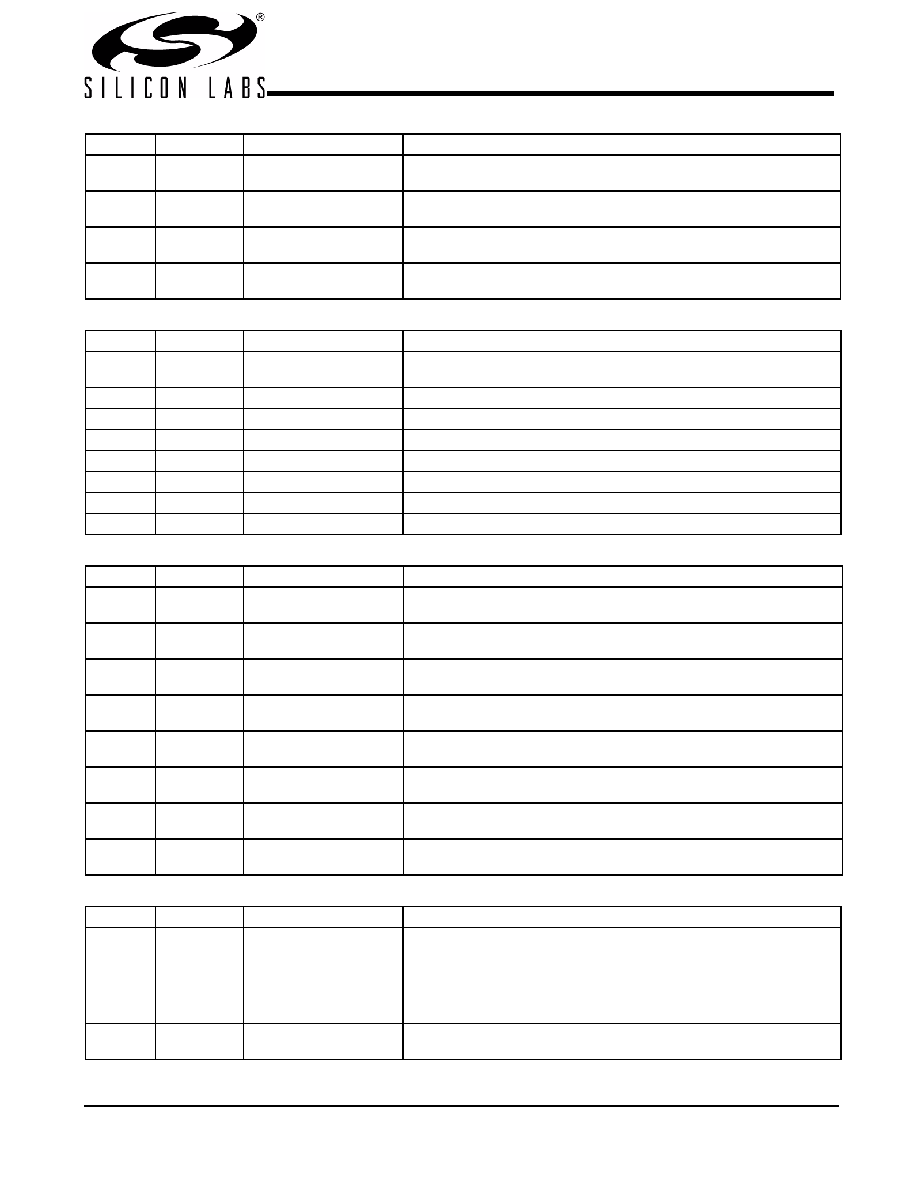
Byte 1: Control Register 1
Bit
@Pup
Name
Description
7
0
SRCT, SRCC
Allows control of SRCT/C with assertion of PCI_STP# or SW PCI_STP
0 = Free Running, 1 = Stopped with PCI_STP#
6
1
SRCT, SRCC
SRCT/C Output Enable; 0 = Disabled (Hi-z), 1 = Enabled
5
1
Reserved
Reserved, Set = 1
4
1
Reserved
Reserved, Set = 1
3
1
Reserved
Reserved, Set = 1
2
1
CPUT2, CPUC2
CPUT/C2 Output Enable; 0 = Disabled (Hi-z), 1 = Enabled
1
CPUT1, CPUC1
CPUT/C1 Output Enable; 0 = Disabled (Hi-z), 1 = Enabled
0
1
CPUT0, CPUC0
CPUT/C0 Output Enable; 0 = Disabled (Hi-z), 1 = Enabled
Byte 2: Control Register 2
Bit
@Pup
Name
Description
7
0
SRCT, SRCC
SRCT/C Pwrdwn Drive Mode
0 = Driven during power-down, 1 = Three-state during power-down
6
0
SRCT, SRCC
SRCT/C Stop Drive Mode
0 = Driven during PCI_STP, 1 = Three-state during PCI_STP
5
0
CPUT2, CPUC2
CPUT/C2 Pwrdwn Drive Mode
0 = Driven during power-down, 1 = Three-state during power-down
4
0
CPUT1, CPUC1
CPUT/C1 Pwrdwn Drive Mode
0 = Driven during power-down, 1 = Three-state during power-down
3
0
CPUT0, CPUC0
CPUT/C0 Pwrdwn Drive Mode
0 = Driven during power-down, 1 = Three-state during power-down
2
0
CPUT2, CPUC2
CPUT/C2 stop Drive Mode
0 = Driven when stopped, 1 = Three-state when stopped
1
0
CPUT1, CPUC1
CPUT/C1 stop Drive Mode
0 = Driven when stopped, 1 = Three-state when stopped
0
CPUT0, CPUC0
CPUT/C0 stop Drive Mode
0 = Driven when stopped, 1 = Three-state when stopped
Byte 3: Control Register 3
Bit
@Pup
Name
Description
7
1
SW PCI STOP
SW PCI_STP Function
0= PCI_STP assert, 1= PCI_STP deassert
When this bit is set to 0, all STOPPABLE PCI, PCIF and SRC outputs will
be stopped in a synchronous manner with no short pulses.
When this bit is set to 1, all STOPPED PCI,PCIF and SRC outputs will
resume in a synchronous manner with no short pulses.
6
1
PCI6
PCI6 Output Enable
0 = Disabled, 1 = Enabled
Byte 0:Control Register 0 (continued)
Bit
@Pup
Name
Description
相關(guān)PDF資料 |
PDF描述 |
|---|---|
| VE-B4B-MW-F3 | CONVERTER MOD DC/DC 95V 100W |
| VE-JTJ-MZ-F2 | CONVERTER MOD DC/DC 36V 25W |
| VE-JTJ-MZ-F1 | CONVERTER MOD DC/DC 36V 25W |
| VE-B4B-MW-F2 | CONVERTER MOD DC/DC 95V 100W |
| AD5315ARMZ-REEL7 | IC DAC 10BIT OCTAL W/BUF 10-MSOP |
相關(guān)代理商/技術(shù)參數(shù) |
參數(shù)描述 |
|---|---|
| CY28409ZXCT | 功能描述:時鐘合成器/抖動清除器 SysClk Intel Grntsdl 865 and 875 chipsets RoHS:否 制造商:Skyworks Solutions, Inc. 輸出端數(shù)量: 輸出電平: 最大輸出頻率: 輸入電平: 最大輸入頻率:6.1 GHz 電源電壓-最大:3.3 V 電源電壓-最小:2.7 V 封裝 / 箱體:TSSOP-28 封裝:Reel |
| CY28410 | 制造商:SPECTRALINEAR 制造商全稱:SPECTRALINEAR 功能描述:Clock Generator for Intel Grantsdale Chipset |
| CY28410-2 | 制造商:CYPRESS 制造商全稱:Cypress Semiconductor 功能描述:Clock Generator for Intel Grantsdale Chipset |
| CY284108OXC | 功能描述:時鐘發(fā)生器及支持產(chǎn)品 Server, CK410B RoHS:否 制造商:Silicon Labs 類型:Clock Generators 最大輸入頻率:14.318 MHz 最大輸出頻率:166 MHz 輸出端數(shù)量:16 占空比 - 最大:55 % 工作電源電壓:3.3 V 工作電源電流:1 mA 最大工作溫度:+ 85 C 安裝風(fēng)格:SMD/SMT 封裝 / 箱體:QFN-56 |
| CY284108OXCT | 功能描述:時鐘發(fā)生器及支持產(chǎn)品 Server, CK410B RoHS:否 制造商:Silicon Labs 類型:Clock Generators 最大輸入頻率:14.318 MHz 最大輸出頻率:166 MHz 輸出端數(shù)量:16 占空比 - 最大:55 % 工作電源電壓:3.3 V 工作電源電流:1 mA 最大工作溫度:+ 85 C 安裝風(fēng)格:SMD/SMT 封裝 / 箱體:QFN-56 |
發(fā)布緊急采購,3分鐘左右您將得到回復(fù)。