- 您現(xiàn)在的位置:買賣IC網(wǎng) > PDF目錄382920 > CS9203 PDF資料下載
參數(shù)資料
| 型號(hào): | CS9203 |
| 文件頁(yè)數(shù): | 5/8頁(yè) |
| 文件大小: | 66K |
| 代理商: | CS9203 |

CS9202
http://onsemi.com
5
CALCULATING POWER DISSIPATION IN A
SINGLE OUTPUT LINEAR REGULATOR
The maximum power dissipation for a single output
regulator (Figure 8) is:
PD(max)
{VIN(max)
VIN(max)IQ
VOUT(min)} IOUT(max)
(1)
where:
V
IN(max)
is the maximum input voltage,
V
OUT(min)
is the minimum output voltage,
I
OUT(max)
is the maximum output current for the
application, and
I
Q
is the quiescent current the regulator consumes at
I
OUT(max)
.
Once the value of P
D(max)
is known, the maximum
permissible value of R
Θ
JA
can be calculated:
150
°
C
R JA
TA
PD
(2)
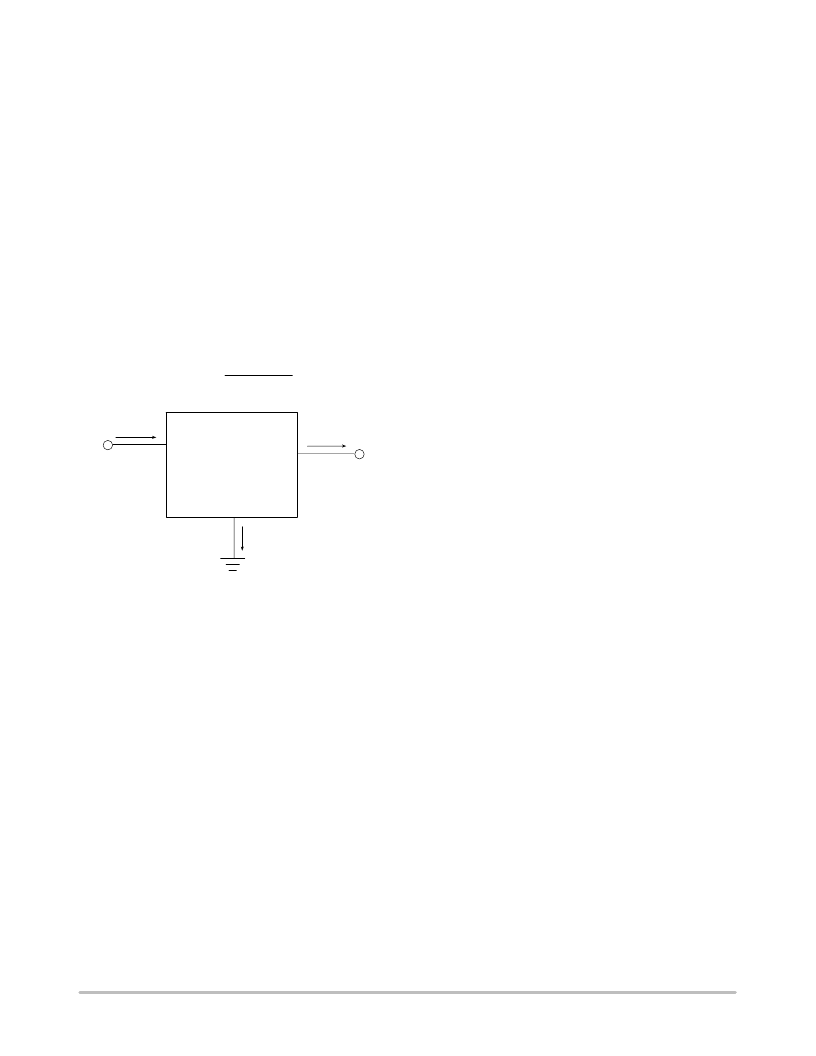
Figure 8. Single output regulator with key
performance parameters labeled.
I
IN
I
OUT
I
Q
CS9202
V
OUT
V
IN
The value of R
Θ
JA
can then be compared with those in the
package section of the data sheet. Those packages with
R
Θ
JA
’s less than the calculated value in equation 2 will keep
the die temperature below 150
°
C
.
In some cases, none of the packages will be sufficient to
dissipate the heat generated by the IC, and an external
heatsink will be required.
HEAT SINKS
A heat sink effectively increases the surface area of the
package to improve the flow of heat away from the IC and
into the surrounding air.
Each material in the heat flow path between the IC and the
outside environment will have a thermal resistance. Like
series electrical resistances, these resistances are summed to
determine the value of R
Θ
JA
:
R JA
R JC
where:
R
Θ
JC
= the junction–to–case thermal resistance,
R
Θ
CS
= the case–to–heatsink thermal resistance, and
R
Θ
SA
= the heatsink–to–ambient thermal resistance.
R CS
R SA
(3)
R
Θ
JC
appears in the package section of the data sheet.
Like R
Θ
JA
, it too is a function of package type. R
Θ
CS
and
R
Θ
SA
are functions of the package type, heatsink and the
interface between them. These values appear in heat sink
data sheets of heat sink manufacturers.
相關(guān)PDF資料 |
PDF描述 |
|---|---|
| CS9203-CL | Sound Generator Circuit |
| CS92210 | CS92210 Product Bulletin|MPEG-2 VIDEO Encoder/Decoder| |
| CS92288 | Peripheral IC |
| CS9233 | Analog IC |
| CS92 | Series: Silicon Controlled Rectifier 0.8 Amps 100 thru 800 Volts JEDEC TO |
相關(guān)代理商/技術(shù)參數(shù) |
參數(shù)描述 |
|---|---|
| CS9203-CL | 制造商:CRYSTAL 功能描述: 制造商:CRYSTAL 功能描述:SOUND GENERATOR CIRCUIT, 68 Pin, PLCC |
| CS9210 | 制造商:NSC 制造商全稱:National Semiconductor 功能描述:Geode⑩ CS9210 Graphics Companion DSTN Controller |
| CS9210-VNG | 制造商:NSC 制造商全稱:National Semiconductor 功能描述:Geode⑩ CS9210 Graphics Companion DSTN Controller |
| CS9211 | 制造商:NSC 制造商全稱:National Semiconductor 功能描述:Geode CS9211 Graphics Companion Flat Panel Display Controller |
| CS9211-VNG | 制造商:Texas Instruments 功能描述: 制造商:National Semiconductor Corporation 功能描述:1024 X 768 PIXELS CRT OR FLAT PNL GRPH DSPL CTLR, PQFP144 |
發(fā)布緊急采購(gòu),3分鐘左右您將得到回復(fù)。