- 您現(xiàn)在的位置:買賣IC網(wǎng) > PDF目錄374167 > CS5157HGD16 (ZF Electronics Corporation) CPU 5-Bit Synchronous Buck Controller PDF資料下載
參數(shù)資料
| 型號(hào): | CS5157HGD16 |
| 廠商: | ZF Electronics Corporation |
| 英文描述: | CPU 5-Bit Synchronous Buck Controller |
| 中文描述: | CPU的5位同步降壓控制器 |
| 文件頁數(shù): | 11/14頁 |
| 文件大小: | 316K |
| 代理商: | CS5157HGD16 |
C
Applications Information: continued
11
used as the source for the regulator output current, the fol-
lowing gate drive is provided;
V
GATE(H)
= 12V - 5V = 7V, V
GATE(L)
= 12V (see Figure 17).
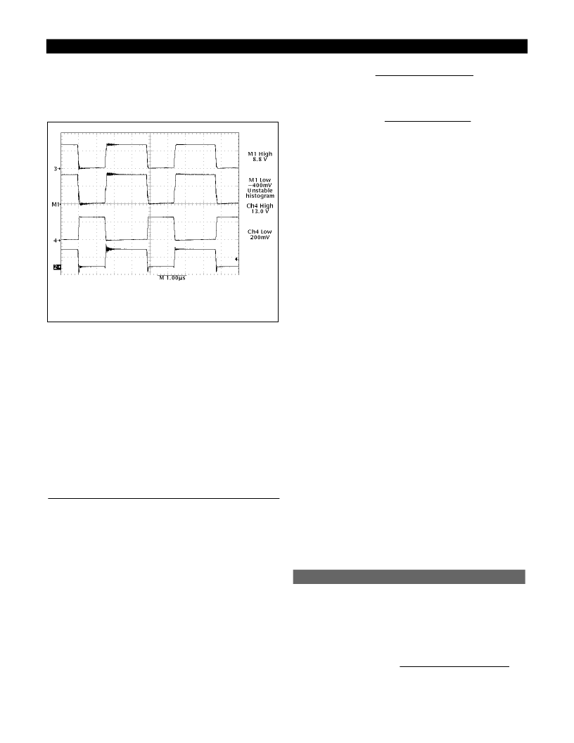
Figure 17: CS5157 gate drive waveforms depicting rail to rail swing.
The most important aspect of MOSFET performance is
RDS
ON
, which effects regulator efficiency and MOSFET
thermal management requirements.
The power dissipated by the MOSFETs may be estimated
as follows;
Switching MOSFET:
Power = I
LOAD2
×
RDS
ON
×
duty cycle
Synchronous MOSFET:
Power = I
LOAD2
×
RDS
ON
×
(1 - duty cycle)
Duty Cycle =
Off Time Capacitor (C
OFF
)
The C
OFF
timing capacitor sets the regulator off time:
T
OFF
= C
OFF
×
4848.5
When the V
FFB
pin is less than 1V, the current charging the
C
OFF
capacitor is reduced. The extended off time can be cal-
culated as follows:
T
OFF
= C
OFF
×
24,242.5.
Off time will be determined by either the T
OFF
time, or the
time out timer, whichever is longer.
The preceding equations for duty cycle can also be used to
calculate the regulator switching frequency and select the
C
OFF
timing capacitor:
C
OFF
=
,
where:
Period =
Schottky Diode for Synchronous MOSFET
A Schottky diode may be placed in parallel with the syn-
chronous MOSFET to conduct the inductor current upon
turn off of the switching MOSFET to improve efficiency.
The CS5157 reference circuit does not use this device due to
it’s excellent design. Instead, the body diode of the syn-
chronous MOSFET is utilized to reduce cost and conducts
the inductor current. For a design operating at 200kHz or so,
the low non-overlap time combined with Schottky forward
recovery time may make the benefits of this device not
worth the additional expense (see Figure 6, channel 2). The
power dissipation in the synchronous MOSFET due to body
diode conduction can be estimated by the following equation:
Power = V
bd
×
I
LOAD
×
conduction time
×
switching frequency
Where V
bd
= the forward drop of the MOSFET body diode.
For the CS5157 demonstration board as shown in Figure 6;
Power = 1.6V
×
13A
×
100ns
×
233kHz = 0.48W
This is only 1.3% of the 36.4W being delivered to the load.
Input and Output Capacitors
These components must be selected and placed carefully to
yield optimal results. Capacitors should be chosen to pro-
vide acceptable ripple on the input supply lines and regula-
tor output voltage. Key specifications for input capacitors
are their ripple rating, while ESR is important for output
capacitors. For best transient response, a combination of
low value/high frequency and bulk capacitors placed close
to the load will be required.
Output Inductor
The inductor should be selected based on its inductance,
current capability, and DC resistance. Increasing the induc-
tor value will decrease output voltage ripple, but degrade
transient response.
Thermal Considerations for Power MOSFETs and Diodes
In order to maintain good reliability, the junction tempera-
ture of the semiconductor components should be kept to a
maximum of 150°C or lower. The thermal impedance (junc-
tion to ambient) required to meet this requirement can be
calculated as follows:
Thermal Impedance = T
JUNCTION(MAX)
- T
AMBIENT
Power
Thermal Management
1
switching frequency
Period
×
(1 - duty cycle)
4848.5
V
OUT
+ (I
LOAD
×
RDS
ON OF SYNCH FET
)
V
IN
+ (I
LOAD
×
RDS
ON OF SYNCH FET
) - (I
LOAD
×
RDS
ON OF SWITCH FET
)
Trace 3 = V
GATE(H)
(10V/div.)
Math 1= V
GATE(H)
- 5V
Trace 4 = V
(10V/div.)
Trace 2 = Inductor Switching Node (5V/div.)
相關(guān)PDF資料 |
PDF描述 |
|---|---|
| CS5157HGDR16 | CPU 5-Bit Synchronous Buck Controller |
| CS5158 | CPU 5-Bit Synchronous Buck Controller |
| CS5158GD16 | CPU 5-Bit Synchronous Buck Controller |
| CS5158GDR16 | CPU 5-Bit Synchronous Buck Controller |
| CS5165GDW16 | Fast, Precise 5-Bit Synchronous Buck Controller for the Next Generation Low Voltage Pentium II Processors |
相關(guān)代理商/技術(shù)參數(shù) |
參數(shù)描述 |
|---|---|
| CS5157HGD16G | 功能描述:DC/DC 開關(guān)控制器 5-Bit Synchronous Dual N-Channel Buck RoHS:否 制造商:Texas Instruments 輸入電壓:6 V to 100 V 開關(guān)頻率: 輸出電壓:1.215 V to 80 V 輸出電流:3.5 A 輸出端數(shù)量:1 最大工作溫度:+ 125 C 安裝風(fēng)格: 封裝 / 箱體:CPAK |
| CS5157HGDR16 | 功能描述:DC/DC 開關(guān)控制器 5-Bit Synchronous RoHS:否 制造商:Texas Instruments 輸入電壓:6 V to 100 V 開關(guān)頻率: 輸出電壓:1.215 V to 80 V 輸出電流:3.5 A 輸出端數(shù)量:1 最大工作溫度:+ 125 C 安裝風(fēng)格: 封裝 / 箱體:CPAK |
| CS5157HGDR16G | 功能描述:DC/DC 開關(guān)控制器 5-Bit Synchronous Dual N-Channel Buck RoHS:否 制造商:Texas Instruments 輸入電壓:6 V to 100 V 開關(guān)頻率: 輸出電壓:1.215 V to 80 V 輸出電流:3.5 A 輸出端數(shù)量:1 最大工作溫度:+ 125 C 安裝風(fēng)格: 封裝 / 箱體:CPAK |
| CS-5158D16 | 制造商:未知廠家 制造商全稱:未知廠家 功能描述:Voltage-Mode SMPS Controller |
| CS-5158DR16 | 制造商:未知廠家 制造商全稱:未知廠家 功能描述:Voltage-Mode SMPS Controller |
發(fā)布緊急采購,3分鐘左右您將得到回復(fù)。