- 您現(xiàn)在的位置:買賣IC網(wǎng) > PDF目錄374167 > CS5155H (ZF Electronics Corporation) CPU 5-Bit Synchronous Buck Controller PDF資料下載
參數(shù)資料
| 型號: | CS5155H |
| 廠商: | ZF Electronics Corporation |
| 英文描述: | CPU 5-Bit Synchronous Buck Controller |
| 中文描述: | CPU的5位同步降壓控制器 |
| 文件頁數(shù): | 5/14頁 |
| 文件大小: | 279K |
| 代理商: | CS5155H |
5
C
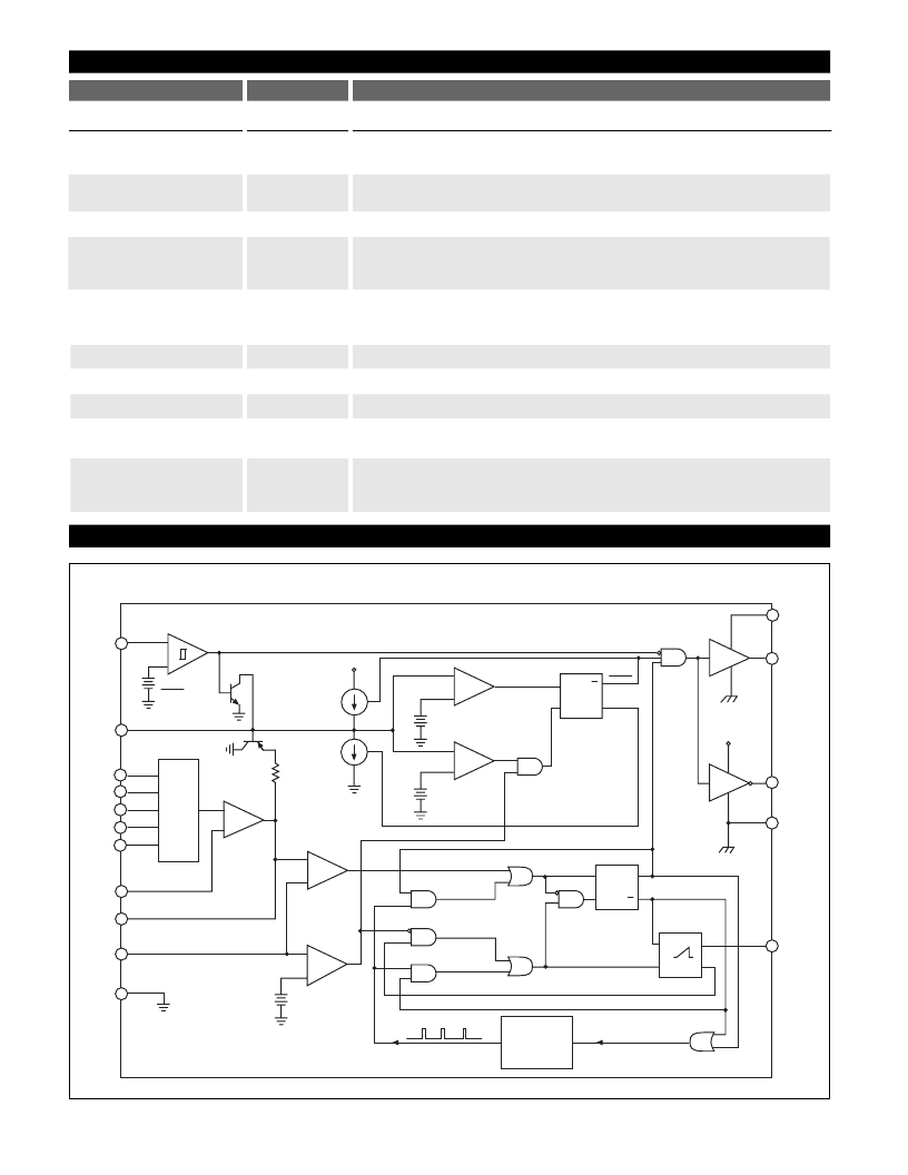
Block Diagram
Q
V
ID1
V
CC1
SS
COMP
V
FB
V
ID0
LGnd
V
FFB
V
CC2
V
GATE(H)
PGnd
V
GATE(L)
V
ID2
V
ID3
-
+
5 BIT
DAC
C
OFF
Slow Feedback
Maximum
On-Time
Timeout
V
CC1
R
Q
S
C
One Shot
PWM
COMP
SS High
Comparator
FAULT
Latch
2.5V
Error
Amplifier
Fast Feedback
-
+
V
CC1
Monitor
Comparator
V
ID4
-
+
-
+
-
+
-
+
V
Low
Comparator
PWM
Comparator
SS Low
Comparator
R
Q
S
Q
R
Q
S
2
m
A
5V
60
m
A
Normal
Off-Time
Timeout
Extended
Off-Time
Timeout
Time Out
Timer
(30
m
s)
Edge Triggered
Off-Time
Timeout
3.90V
3.85V
FAULT
FAULT
GATE(H) = ON
GATE(H) = OFF
PGnd
PWM
Latch
1V
0.7V
Package Pin Description: continued
PACKAGE PIN #
PIN SYMBOL
FUNCTION
16L SO Narrow & PDIP
7
C
OFF
A capacitor from this pin to ground sets the time duration for the on
board one shot, which is used for the constant off time architecture.
8
V
FFB
Fast feedback connection to the PWM comparator. This pin is connect-
ed to the regulator output. The inner feedback loop terminates on time.
9
V
CC2
V
GATE(H)
Boosted power for the high side gate driver.
10
High FET driver pin capable of 1.5A peak switching current. Internal
circuit prevents V
GATE(H)
and V
GATE(L)
from being in high state simul-
taneously.
11
PGnd
High current ground for the IC. The MOSFET drivers are referenced to
this pin. Input capacitor ground and the source of lower FET should be
tied to this pin.
12
V
GATE(L)
V
CC1
LGnd
Low FET driver pin capable of 1.5A peak switching current.
13
Input power for the IC and low side gate driver.
14
Signal ground for the IC. All control circuits are referenced to this pin.
15
COMP
Error amplifier compensation pin. A capacitor to ground should be
provided externally to compensate the amplifier.
16
V
FB
Error amplifier DC feedback input. This is the master voltage feedback
which sets the output voltage. This pin can be connected directly to the
output or a remote sense trace.
相關(guān)PDF資料 |
PDF描述 |
|---|---|
| CS5155GD16 | CPU 5-Bit Synchronous Buck Controller |
| CS5155GN16 | CPU 5-Bit Synchronous Buck Controller |
| CS5156GD16 | CPU 5-Bit Nonsynchronous Buck Controller |
| CS5156GDR16 | CPU 5-Bit Nonsynchronous Buck Controller |
| CS5156 | CPU 5-Bit Nonsynchronous Buck Controller |
相關(guān)代理商/技術(shù)參數(shù) |
參數(shù)描述 |
|---|---|
| CS-5155HD16 | 制造商:未知廠家 制造商全稱:未知廠家 功能描述:Voltage-Mode SMPS Controller |
| CS-5155HDR16 | 制造商:未知廠家 制造商全稱:未知廠家 功能描述:Voltage-Mode SMPS Controller |
| CS-5155HN16 | 制造商:未知廠家 制造商全稱:未知廠家 功能描述:Voltage-Mode SMPS Controller |
| CS5155N16 | 制造商:ON Semiconductor 功能描述: |
| CS-5155N16 | 制造商:未知廠家 制造商全稱:未知廠家 功能描述:Voltage-Mode SMPS Controller |
發(fā)布緊急采購,3分鐘左右您將得到回復(fù)。