- 您現(xiàn)在的位置:買賣IC網(wǎng) > PDF目錄374167 > CS5150GDR16 (ZF Electronics Corporation) CPU 4-Bit Synchronous Buck Controller PDF資料下載
參數(shù)資料
| 型號(hào): | CS5150GDR16 |
| 廠商: | ZF Electronics Corporation |
| 英文描述: | CPU 4-Bit Synchronous Buck Controller |
| 中文描述: | CPU的4位同步降壓控制器 |
| 文件頁數(shù): | 5/14頁 |
| 文件大小: | 322K |
| 代理商: | CS5150GDR16 |
5
C
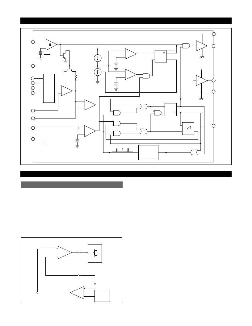
Block Diagram
Q
V
ID1
V
CC1
SS
COMP
V
FB
V
ID0
LGnd
V
FFB
V
CC2
V
GATE(H)
PGnd
V
GATE(L)
V
ID2
V
ID3
-
+
4 BIT
DAC
C
OFF
Slow Feedback
Maximum
On-Time
Timeout
V
CC1
R
Q
S
C
OFF
One Shot
PWM
COMP
SS High
Comparator
FAULT
Latch
2.5V
Error
Amplifier
Fast Feedback
-
+
V
Monitor
Comparator
-
+
-
+
-
+
-
+
V
Low
Comparator
PWM
Comparator
SS Low
Comparator
R
Q
S
Q
R
Q
S
2
μ
A
5V
60
μ
A
Normal
Off-Time
Timeout
Extended
Off-Time
Timeout
Time Out
Timer
(30
μ
s)
Edge Triggered
Off-Time
Timeout
3.90V
3.85V
FAULT
FAULT
GATE(H) = ON
GATE(H) = OFF
PGnd
PWM
Latch
1V
0.7V
Applications Information
V
2
Control Method
The V
2
method of control uses a ramp signal that is gen-
erated by the ESR of the output capacitors. This ramp is
proportional to the AC current through the main inductor
and is offset by the value of the DC output voltage. This
control scheme inherently compensates for variation in
either line or load conditions, since the ramp signal is gen-
erated from the output voltage itself. This control scheme
differs from traditional techniques such as voltage mode,
which generates an artificial ramp, and current mode,
which generates a ramp from inductor current.
Figure 1: V
2
Control Diagram
The V
2
control method is illustrated in Figure 1. The out-
put voltage is used to generate both the error signal and the
ramp signal. Since the ramp signal is simply the output
voltage, it is affected by any change in the output regard-
less of the origin of that change. The ramp signal also con-
tains the DC portion of the output voltage, which allows
the control circuit to drive the main switch to 0% or 100%
duty cycle as required.
A change in line voltage changes the current ramp in the
inductor, affecting the ramp signal, which causes the V
2
control scheme to compensate the duty cycle. Since the
change in inductor current modifies the ramp signal, as in
current mode control, the V
2
control scheme has the
same advantages in line transient response.
A change in load current will have an affect on the output
voltage, altering the ramp signal. A load step immediately
changes the state of the comparator output, which controls
the main switch. Load transient response is determined
only by the comparator response time and the transition
speed of the main switch. The reaction time to an output
load step has no relation to the crossover frequency of the
error signal loop, as in traditional control methods.
The error signal loop can have a low crossover frequency,
since transient response is handled by the ramp signal loop.
The main purpose of this ‘slow’ feedback loop is to provide
DC accuracy. Noise immunity is significantly improved,
since the error amplifier bandwidth can be rolled off at a low
frequency. Enhanced noise immunity improves remote sens-
Reference
Voltage
+
C
–
E
+
–
Ramp
Signal
Output
Voltage
Feedback
Error
Signal
V
GATE(H)
V
GATE(L)
Error
Amplifier
V
FFB
COMP
V
FB
PWM
Comparator
Theory of Operation
相關(guān)PDF資料 |
PDF描述 |
|---|---|
| CS5150 | CPU 4-Bit Synchronous Buck Controller |
| CS5150H | CPU 4-Bit Synchronous Buck Controller |
| CS5150GD16 | CPU 4-Bit Synchronous Buck Controller |
| CS5150GN16 | CPU 4-Bit Synchronous Buck Controller |
| CS5151GN16 | CPU 4-Bit Nonsynchronous Buck Controller |
相關(guān)代理商/技術(shù)參數(shù) |
參數(shù)描述 |
|---|---|
| CS5150GN16 | 制造商:Rochester Electronics LLC 功能描述:- Bulk |
| CS-5150H | 制造商:未知廠家 制造商全稱:未知廠家 功能描述:CPU 4-Bit Synchronous Buck Controller |
| CS-5150HD16 | 制造商:未知廠家 制造商全稱:未知廠家 功能描述:Voltage-Mode SMPS Controller |
| CS-5150HDR16 | 制造商:未知廠家 制造商全稱:未知廠家 功能描述:Voltage-Mode SMPS Controller |
| CS-5150N16 | 制造商:未知廠家 制造商全稱:未知廠家 功能描述:Voltage-Mode SMPS Controller |
發(fā)布緊急采購,3分鐘左右您將得到回復(fù)。