- 您現(xiàn)在的位置:買賣IC網(wǎng) > PDF目錄366892 > CR16MCT9VJE7 Microcontroller PDF資料下載
參數(shù)資料
| 型號: | CR16MCT9VJE7 |
| 英文描述: | Microcontroller |
| 中文描述: | 微控制器 |
| 文件頁數(shù): | 140/157頁 |
| 文件大小: | 1256K |
| 代理商: | CR16MCT9VJE7 |
第1頁第2頁第3頁第4頁第5頁第6頁第7頁第8頁第9頁第10頁第11頁第12頁第13頁第14頁第15頁第16頁第17頁第18頁第19頁第20頁第21頁第22頁第23頁第24頁第25頁第26頁第27頁第28頁第29頁第30頁第31頁第32頁第33頁第34頁第35頁第36頁第37頁第38頁第39頁第40頁第41頁第42頁第43頁第44頁第45頁第46頁第47頁第48頁第49頁第50頁第51頁第52頁第53頁第54頁第55頁第56頁第57頁第58頁第59頁第60頁第61頁第62頁第63頁第64頁第65頁第66頁第67頁第68頁第69頁第70頁第71頁第72頁第73頁第74頁第75頁第76頁第77頁第78頁第79頁第80頁第81頁第82頁第83頁第84頁第85頁第86頁第87頁第88頁第89頁第90頁第91頁第92頁第93頁第94頁第95頁第96頁第97頁第98頁第99頁第100頁第101頁第102頁第103頁第104頁第105頁第106頁第107頁第108頁第109頁第110頁第111頁第112頁第113頁第114頁第115頁第116頁第117頁第118頁第119頁第120頁第121頁第122頁第123頁第124頁第125頁第126頁第127頁第128頁第129頁第130頁第131頁第132頁第133頁第134頁第135頁第136頁第137頁第138頁第139頁當前第140頁第141頁第142頁第143頁第144頁第145頁第146頁第147頁第148頁第149頁第150頁第151頁第152頁第153頁第154頁第155頁第156頁第157頁
www.national.com
140
Output Signal Levels
All output signals are powered by the digital supply (VCC).
Table 44 summarizes the states of the output signals during
the reset state (when VCC power exists in the reset state)
and during the Power Save mode.
The RESET and NMI input pins are active during the Power
Save mode. In order to guarantee that the Power Save cur-
rent not exceed 1mA, these inputs must be driven to a volt-
age lower than 0.5V or higher than VCC-0.5V. An input
voltage between 0.5V and (VCC-0.5V) may result in power
consumption exceeding 1 mA.
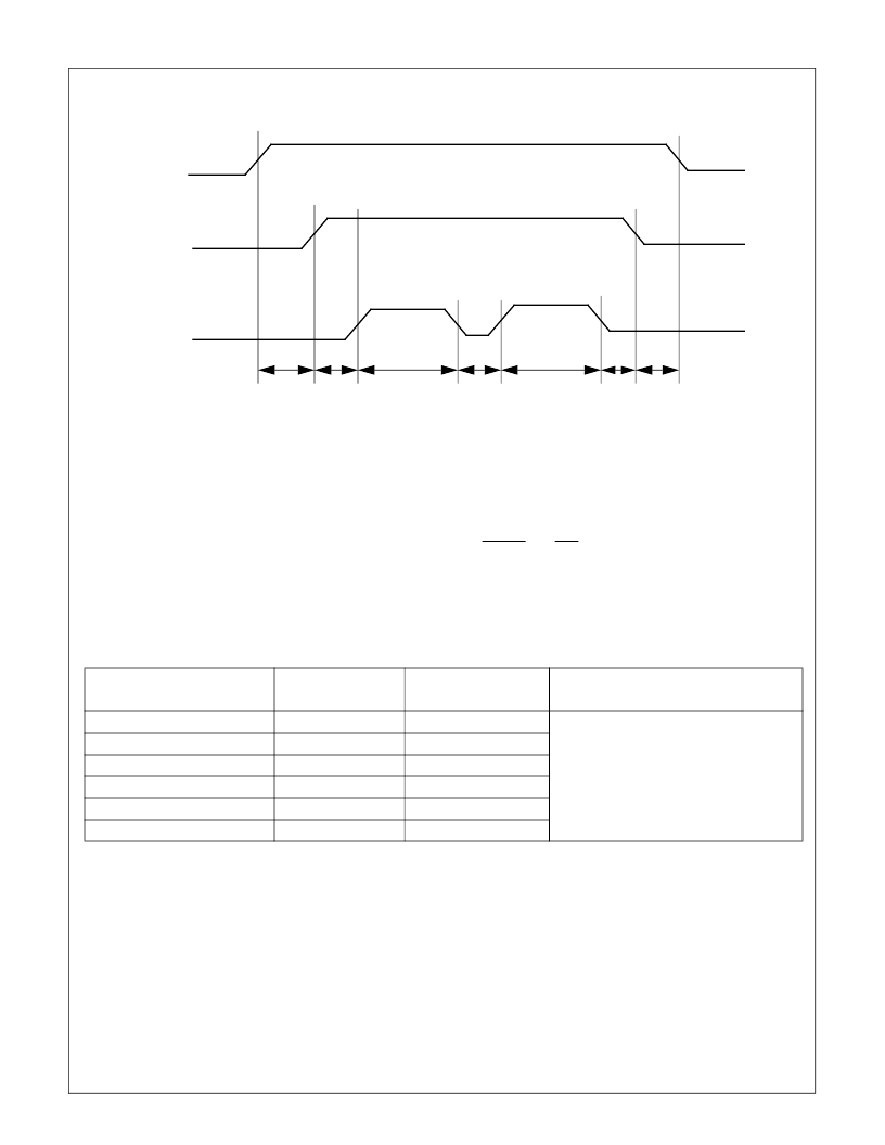
Output Pins During Reset and Power-Save
t
SD
t
TT
t
PW
t
PW
t
PE
t
ED
t
PP
Row Select/
Start Charge
Pump
Select
Charge Pump/
Enable
Programming
Voltage
Programming
Pulse
Figure 76.
Flash EEPROM Memory Programming Timing
(Sample Sequence for Programming two Words into Flash EEPROM Program Memory
Table 44
Signals on a pin
Reset state
(with Vcc)
Power Save mode
Comments
PF[0:7]
PG[0:7]
PI[0:7]
PL[0:7]
PB[0:7]
PC[0:7]
TRI-STATE
TRI-STATE
TRI-STATE
TRI-STATE
TRI-STATE
TRI-STATE
Previous state
Previous state
Previous state
Previous state
Previous state
Previous state
I/O ports will maintain their values when
entering power-save mode
相關PDF資料 |
PDF描述 |
|---|---|
| CR16MCT9VJE7Y | Microcontroller |
| CR16MCT9VJE8 | Microcontroller |
| CR16MCT9VJE8Y | Microcontroller |
| CR16MCT9VJE9 | Microcontroller |
| CR16MCT9VJE9Y | Microcontroller |
相關代理商/技術參數(shù) |
參數(shù)描述 |
|---|---|
| CR16MCT9VJE7Y | 制造商:未知廠家 制造商全稱:未知廠家 功能描述:Microcontroller |
| CR16MCT9VJE8 | 制造商:未知廠家 制造商全稱:未知廠家 功能描述:Microcontroller |
| CR16MCT9VJE8Y | 制造商:未知廠家 制造商全稱:未知廠家 功能描述:Microcontroller |
| CR16MCT9VJE9 | 制造商:未知廠家 制造商全稱:未知廠家 功能描述:Microcontroller |
| CR16MCT9VJE9Y | 制造商:未知廠家 制造商全稱:未知廠家 功能描述:Microcontroller |
發(fā)布緊急采購,3分鐘左右您將得到回復。