- 您現(xiàn)在的位置:買賣IC網(wǎng) > PDF目錄384225 > CM8872CPEI-1 DTMF Receiver PDF資料下載
參數(shù)資料
| 型號: | CM8872CPEI-1 |
| 英文描述: | DTMF Receiver |
| 中文描述: | 雙音多頻接收器 |
| 文件頁數(shù): | 3/9頁 |
| 文件大?。?/td> | 76K |
| 代理商: | CM8872CPEI-1 |
200
1
California Micro Devices Corp. All rights reserved.
1
2
/
18
/2001
3
215 Topaz Street, Milpitas, California 95035
Tel: (408) 263-3214
Fax: (408) 263-7846
www.calmicro.com
CM8870/70C
CALIFORNIA MICRO DEVICES
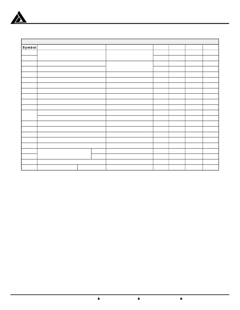
AC Characteristics
Notes
1, 2, 3, 4, 5, 8
2, 3, 4, 8
2, 3, 5, 8, 10
2, 3, 5
2, 3, 4, 5, 8, 9, 13, 14
2, 3, 4, 5, 6, 8, 9
2, 3, 4,5, 7, 8, 9
Refer to Timing Diagram
Refer to Timing Diagram
15
15
15
15
TOE = V
DD
TOE = V
DD
TOE = V
DD
Enable
R
= 10K
Disable
C
L
= 50pf
Capacitive Load
Parameter
MIN
–
29
27.5
±3.5%
5
0.5
20
20
3.5759
TYP
–
16
–
12
22
8
3
6
9
3.4
50
300
3.5795
MAX
1
869
10
10
UNIT
dBm
mV
RMS
dB
dB
Norm.
Norm.
dB
dB
dB
ms
ms
ms
ms
ms
μs
μs
μs
μs
ns
ns
MHz
pF
t
DP
t
DA
t
REC
t
ID
t
DO
t
PQ
t
PS
t
D
t
QS
t
D
t
PTE
t
PTD
f
CLK
C
LO
Valid Input Signal Levels
(each tone of composite signal)
Positive Twist Accept
Negative Twist Accept
Freq. Deviation Aceept Limit
Freq. Deviation Reject Limit
Third Tone Tolerance
Noise Tolerance
Dial Tone Tolerance
Tone Present Detection Time
Tone Absent Dectection Time
MIN Tone Duration Accept
MAX Tone Duration Reject
MIN Interdigit Pause Accept
MAX Interdigit Pause Reject
Propagation Delay (St to Q)
Propagation Delay (St to StD)
Output Data Set Up (Q to StD)
1.5%±2Hz
14
8.5
40
40
11
16
3.5831
30
Propagation Delay (TOE to Q)
Crystal/Clock Frequency
Clock Ouput (OSC 2)
AC Characteristics:
All voltages referenced to V
, V
DD
= 5.0V ±5%, T
A
=
–
40
°
C to +85
°
C, f
CLK
= 3.579545 MHz
using test circuit in Figure 1 unless otherwise noted.
Notes:
1. dBm = decibels above or below a reference power
of 1mW into a 600
load.
2. Digit sequence consists of all 16 DTMF tones.
3. Tone duration = 40ms. Tone pause = 40ms.
4. Nominal DTMF frequencies are used.
5. Both tones in the composite signal have
an equal amplitude.
6. Bandwidth limited (0 to 3KHz) Gaussian Noise.
7. The precise dial tone frequencies are
(350Hz and 440Hz) ±2%.
8. For an error rate of better than 1 in 10,000
9. Referenced to lowest level frequency component
in DTMF signal.
10. Minimum signal acceptance level is measured with
specified maximum frequency deviation.
11. Input pins defined as IN+, IN
–
, and TOE.
12. External voltage source used to bias V
.
13. This parameter also applies to a third tone injected onto
the power supply.
14. Referenced to Figure 1. Input DTMF tone level
at
–
28dBm.
15.Times shown are obtained with circuit in
Figure 1 (User adjustable).
相關(guān)PDF資料 |
PDF描述 |
|---|---|
| CM8872CPI | DTMF Receiver |
| CM8872CPI-1 | DTMF Receiver |
| CM8872CS | DTMF Receiver |
| CM8872CS-1 | DTMF Receiver |
| CM8872CSI | DTMF Receiver |
相關(guān)代理商/技術(shù)參數(shù) |
參數(shù)描述 |
|---|---|
| CM8872CPI | 制造商:未知廠家 制造商全稱:未知廠家 功能描述:DTMF Receiver |
| CM8872CPI-1 | 制造商:未知廠家 制造商全稱:未知廠家 功能描述:DTMF Receiver |
| CM8872CS | 制造商:未知廠家 制造商全稱:未知廠家 功能描述:DTMF Receiver |
| CM8872CS-1 | 制造商:未知廠家 制造商全稱:未知廠家 功能描述:DTMF Receiver |
| CM8872CSI | 制造商:未知廠家 制造商全稱:未知廠家 功能描述:DTMF Receiver |
發(fā)布緊急采購,3分鐘左右您將得到回復(fù)。