- 您現(xiàn)在的位置:買賣IC網(wǎng) > PDF目錄384208 > CL7160EQC160-15 Laser-Programmable Complex PLD PDF資料下載
參數(shù)資料
| 型號(hào): | CL7160EQC160-15 |
| 英文描述: | Laser-Programmable Complex PLD |
| 中文描述: | 激光可編程復(fù)雜可編程邏輯器件 |
| 文件頁(yè)數(shù): | 11/14頁(yè) |
| 文件大小: | 177K |
| 代理商: | CL7160EQC160-15 |
第1頁(yè)第2頁(yè)第3頁(yè)第4頁(yè)第5頁(yè)第6頁(yè)第7頁(yè)第8頁(yè)第9頁(yè)第10頁(yè)當(dāng)前第11頁(yè)第12頁(yè)第13頁(yè)第14頁(yè)
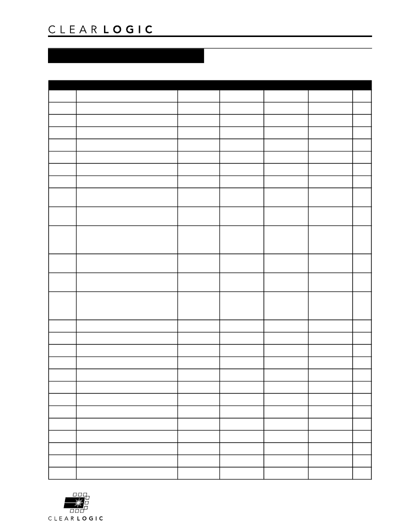
CL7160E and CL7160S Laser Processed Logic Devices
Page 11
Parameter
Conditions
Min
Max
Min
Max
Min
Max
Unit
t
iN
Input pad and buffer delay
0.5
0.5
2.0
ns
t
IO
I/O input pad and buffer delay
0.5
0.5
2.0
ns
t
FIN
Fast input delay
1.0
1.0
1.0
ns
t
SEXP
Shared expander delay
5.0
5.0
7.0
ns
t
PEXP
Parallel expander delay
0.8
0.8
1.0
ns
t
LAD
Logic array delay
5.0
5.0
5.0
ns
t
LAC
Logic control array delay
5.0
5.0
5.0
ns
t
IOE
Internal output enable delay
2.0
2.0
2.0
ns
Output buffer and pad delay
Slow slew rate = off, V
CCIO
= 5.0 V
Output buffer and pad delay
Slow slew rate = off, V
CCIO
= 3.3 V
Output buffer and pad delay
Slow slew rate = on,
V
CCIO
= 5.0 V or 3.3 V
Output buffer enable delay
Slow slew rate = off, V
CCIO
= 5.0 V
Output buffer enable delay
Slow slew rate = off, V
CCIO
= 3.3 V
Output buffer enable delay
Slow slew rate = on,
V
CCIO
= 5.0 V or 3.3 V
t
XZ
Output buffer disable delay
C
L
= 5 pF
[3]
5.0
5.0
6.0
ns
t
SU
Register setup time
2.0
2.0
4.0
ns
t
H
Register hold time
3.0
3.0
4.0
ns
t
FSU
Register setup time of fast input
3.0
3.0
2.0
ns
t
FH
Register hold time of fast input
0.5
0.5
2.0
ns
t
RD
Register delay
2.0
2.0
1.0
ns
t
COMB
Combinatorial delay
2.0
2.0
1.0
ns
t
IC
Array clock delay
5.0
5.0
5.0
ns
t
EN
Register enable time
5.0
5.0
5.0
ns
t
GLOB
Global control delay
1.0
1.0
0.0
ns
t
PRE
Register preset time
3.0
3.0
3.0
ns
t
CLR
Register clear time
3.0
3.0
3.0
ns
t
LIA
LIA delay
1.0
1.0
1.0
ns
5.5
9.0
10.0
5.5
7K tbl 07C2
ns
ns
3.0
7.0
ns
6.0
ns
7.0
2.0
1.5
ns
2.0
4.0
ns
1.5
9.0
5.5
5.0
5.5
5.0
C
L
= 35 pF
C
L
= 35 pF
C
L
= 35 pF
C
L
= 35 pF
t
ZX3
C
L
= 35 pF
C
L
= 35 pF
t
ZX1
t
ZX2
t
OD3
Speed: -10P
Speed: -10
Symbol
Speed: -12
t
OD1
t
OD2
AC Electrical Specifications cont.
Internal Timing Parameters
[4]
相關(guān)PDF資料 |
PDF描述 |
|---|---|
| CL7160EQC160-20 | Laser-Programmable Complex PLD |
| CL7160EQC160-6 | Laser-Programmable Complex PLD |
| CL7160EQI100-15 | Laser-Programmable Complex PLD |
| CL7192SQI160-10 | Laser-Programmable Complex PLD |
| CL7192EQC160-12 | |
相關(guān)代理商/技術(shù)參數(shù) |
參數(shù)描述 |
|---|---|
| CL7163-000 | 制造商:TE Connectivity 功能描述:44A9748-20-9-9CS3185 - Cable Rools/Shrink Tubing |
| CL7174-000 | 制造商:TE Connectivity 功能描述:Heat Shrink Tubing 制造商:TE Connectivity 功能描述:202K121-25-01/225-0-CS8387 - Bulk |
| CL72001X | 制造商:BANDRIDGE 功能描述:LEAD AV CAT5 0.5M |
| CL72002X | 制造商:BANDRIDGE 功能描述:LEAD AV CAT5 2M |
| CL72003X | 制造商:BANDRIDGE 功能描述:LEAD AV CAT5 3M |
發(fā)布緊急采購(gòu),3分鐘左右您將得到回復(fù)。